You are currently viewing SemiWiki as a guest which gives you limited access to the site. To view blog comments and experience other SemiWiki features you must be a registered member. Registration is fast, simple, and absolutely free so please,
join our community today!
WP_Term Object
(
    [term_id] => 18
    [name] => Intel
    [slug] => intel
    [term_group] => 0
    [term_taxonomy_id] => 18
    [taxonomy] => category
    [description] =>
    [parent] => 158
    [count] => 418
    [filter] => raw
    [cat_ID] => 18
    [category_count] => 418
    [category_description] =>
    [cat_name] => Intel
    [category_nicename] => intel
    [category_parent] => 158
    [is_post] =>
)
This will be the year of the semiconductor foundry ecosystem, absolutely. Right in between the Samsung SAFE Forum and the TSMC OIP Open Ecosystem Forum, Intel Foundry Services (IFS) just announced a United States Military, Aerospace, and Government (USMAG) Alliance.
Brilliant move, of course, due to the US Government now being… Read More
The media has gone wild over a false report that Intel and TSMC are slowing down 3nm. It is all about sensationalism and getting clicks no matter what damage is done to the hardworking semiconductor people, companies and industry as a whole. And like lemmings jumping off a cliff, other less reputable media outlets perpetuated this… Read More
Pinpointing exactly when 450mm died is tricky. Intel’s pullback in 2014 has been cited as a pivotal moment because it was the main backer of the proposed transition, as it had been for the shift to 150mm (6-inch) wafers in the early 1980s.
However, the participation of global foundry leader TSMC was also seen as crucial if 450mm wafers… Read More
-Need more/less spend & more/fewer chips
-The irony of chips act passage & Intel stumble on same day
-Due to excess supply of chips, Intel cuts spending
-Due to shortage of chips, the government increases spending
-How did this happen on the same day? Cosmic Coincidence?
Timing is everything
The irony of intel cutting spending… Read More
Most people will be surprised by this but after working in Taiwan for many years I quite expected it. Intel Announced that MediaTek will use Intel Foundry Services for FinFET based smart edge device chips. MediaTek will start with Intel 16nm technology which originated from the legendary 22nm, the first commercial FinFET process.… Read More
3D Device Technology Developmentby Tom Dillinger on 07-13-2022 at 6:00 amCategories: Events, Foundries, Intel
The VLSI Symposium on Technology and Circuits provides a deep dive on recent technical advances, as well as a view into the research efforts that will be transitioning to production in the near future. In a short course presentation at the Symposium, Marko Radosavljevic, from the Components Research group at Intel, provided … Read More
Intel announced today that they are partnering with cloud and EDA companies to better enable their foundry business. This is a natural extension of the Accelerator ecosystem program announced earlier. More and more chip designs are being done in the cloud and from my experience cloud based designs are better. Some companies use… Read More
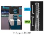
As I previously wrote about here, Intel is presenting their Intel 4 process at the VLSI Technology conference. Last Wednesday Bernhard Sell (Ben) from Intel gave the press a briefing on the process and provided us with early access to the paper (embargoed until Sunday 6/12).
“Intel 4 CMOS Technology Featuring Advanced FinFET Transistors… Read More
From initial process technology development (TD) to high volume manufacturing (HVM) status for a new node, one of the key support functions to improve and maintain yield is the in-line wafer inspection technology. Actually, there are multiple inspection technologies commonly employed, with tradeoffs in pixel resolution,… Read More
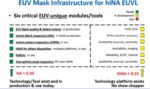
0.55 High-NA Lithography Updateby Tom Dillinger on 05-31-2022 at 6:00 amCategories: Events, Foundries, Intel
At the recent SPIE Advanced Lithography + Patterning Conference, Mark Phillips from Intel gave an insightful update on the status of the introduction of the 0.55 high numerical aperture extreme ultraviolet lithography technology. Mark went so far as to assert that the development progress toward high-NA EUV would support … Read More