The VLSI Symposium on Technology and Circuits provides a deep dive on recent technical advances, as well as a view into the research efforts that will be transitioning to production in the near future. In a short course presentation at the Symposium, Marko Radosavljevic, from the Components Research group at Intel, provided an update on the development status of 3D device fabrication, in a talk entitled “Advanced Logic Scaling Using Monolithic 3D Integration”.
Although there are significant challenges yet to be addressed, Marko provided a compelling perspective that 3D device topologies will be the successor to the emerging gate-all-around (nanosheet/nanoribbon) device. This article summarizes the highlights of Marko’s presentation.
Introduction
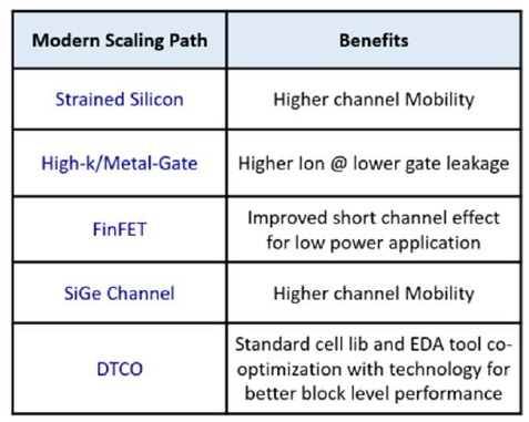
Marko provided a brief recap of recent process technology developments that have led to the current FinFET devices, and to the upcoming GAA topology. The first figure below lists these device scaling features, while the next figure illustrates a cross-sectional view of the FinFET and GAA device stack. (Four vertical nanosheets are illustrated, for the adjacent nFET and pFET devices.)

The GAA topology improves upon the device leakage current control compared to the “tri-gate” surface of the FinFET. (Additional process engineering steps are typically integrated to reduce the substrate surface leakage current for the device gate material between the bottom of the lowest nanosheet and the substrate.)
Also, as depicted in the figure below, the GAA lithography and fabrication offer some flexibility in the width of the nanosheets in the stack. Unlike the quantized width of the FinFET device (w=(2*h)+t), designers will have greater flexibility in optimizing circuits for specific PPA goals.
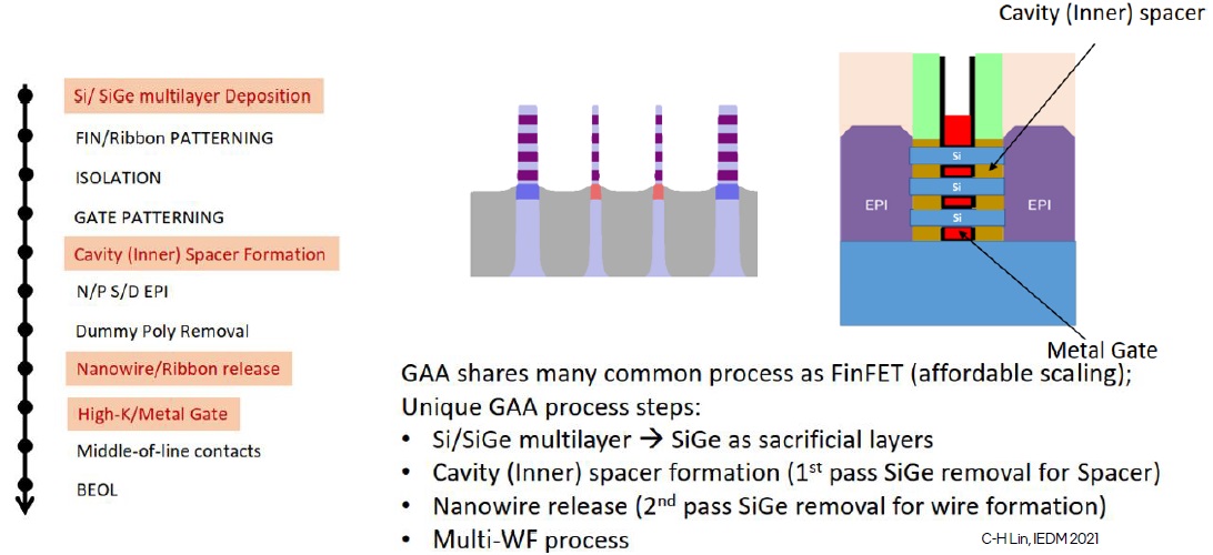
The figure above also highlights some of the GAA process challenges, specifically the steps which are unique compared to FinFET fabrication:
-
- an initial Si/SiGe epitaxial stack
- partial recessed etch of the sacrificial SiGe, exposing the ends of the Si layers for epitaxial growth of the source/drain nodes
FinFETs also use selective epitaxy to expand the S/D nodes – yet, the fins are already exposed on either side of the gate. The GAA device requires a very precise lateral etch of the interspersed SiGe layers to expose the Si surfaces prior to S/D epitaxy.
-
- removal of the remainder of the sacrificial SiGe to “release” the nanosheet surfaces (supported by the S/D epi)
- precise deposition of the gate oxide and surrounding gate metal on all nanosheet surfaces
Note in the figure above that multiple metal gate compositions will be deposited to provide different workfunction surface potentials, for different device Vt thresholds.
3D Devices
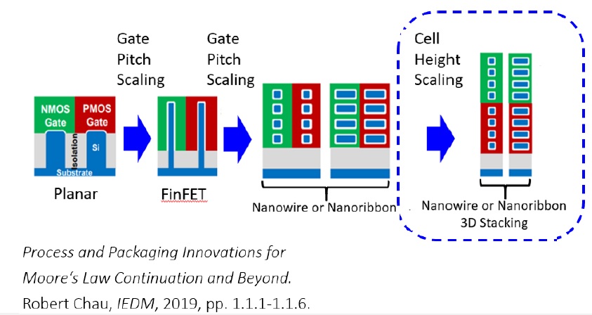
With that background, Marko shared the graphic below, indicating that the next process roadmap device evolution would be to 3D stacked nanoribbons, leveraging the process development experience gained in the lateral pFET and nFET device fabrication. The 3D stacked devices are typically denoted as a “CFET” (complementary FET) structure.
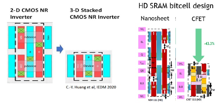
The figure below provides illustrations of how vertical device stacking could have a significant area scaling factor compared to lateral nanosheet layout, both for a logic cell and an SRAM bitcell (a 1-1-1 device configuration for the transfer gate-pullup-pulldown in the 6T cell).
The figure below expands upon the logic inverter layout above, to show the devices in cross-section. Note the presence of buried power rails (BPR) providing VDD and VSS to the devices. Also, note the significant aspect ratios required for contact etch and metal fill.
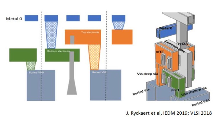
CFET R&D Initiatives
Actually, there are two very distinct approaches being evaluated for fabrication of CFET devices – “sequential” and “monolithic” (or self-aligned).
-
- sequential 3D stacking
The figure below illustrates the sequential process flow. The bottom devices are fabricated first, followed by the bonding of a (thinned) substrate for fabrication of the top devices. An oxide dielectric layer is deposited and polished on the starting substrate for the bonding process and to serve as the electrical isolation between the devices. The presence of the bottom devices constrains the thermal budget available for top device fabrication.
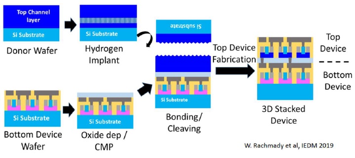
Of particular interest to researchers is that this approach offers the opportunity to utilize different substrate materials (and potentially different device topologies) for the two device types. For example, the figure below shows a (top) pFET fabricated using a nanosheet device in a Ge substrate with a (bottom) nFET using a FinFET structure.
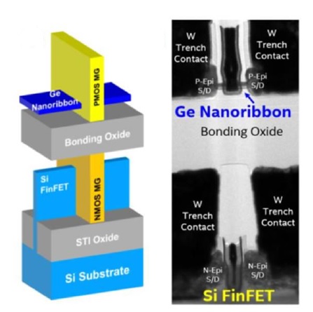
In the example above, the pFETs in the Ge nanosheets would be fabricated using a starting stack of Ge/SiGe layers, with SiGe again serving as the sacrificial support for source/drain growth and nanosheet release. This technology option would leverage the higher hole mobility in Ge compared to Si.
The bonding dielectric thickness separating the two device layers is a key process optimization parameter – a thin layer reduces parasitic interconnect resistances and capacitances, yet needs to be defect-free.
-
- self-aligned monolithic 3D stacking
The figures below illustrate a cross-section of a monolithic self-aligned CFET structure, and a high-level process flow description. (The SiGe layer in the middle is sacrificial.)
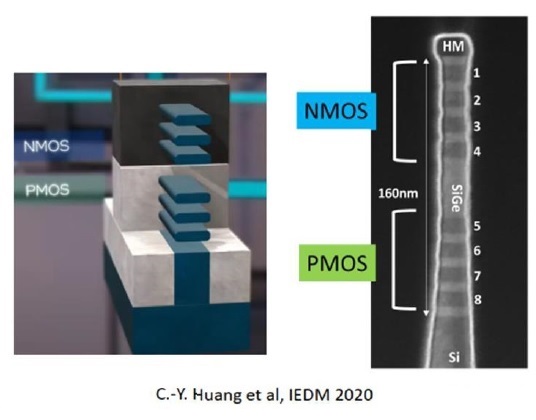
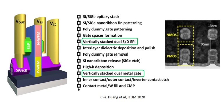
Two key process steps unique to the monolithic vertical device structure that are highlighted in the figure above are the distinct nFET and pFET S/D epitaxy growth and the gate workfunction metal deposition.
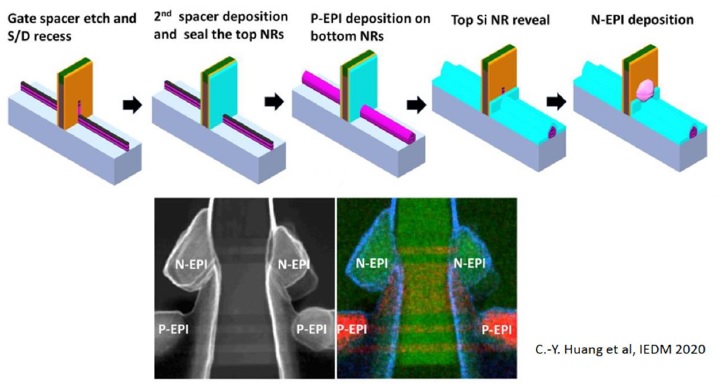
The figure below illustrates S/D epitaxial growth process for the two device types. The top device nanoribbons receive a blocking layer prior to the bottom device S/D epitaxial growth. Then, this blocking layer is removed, the ends of the top nanoribbons are revealed, and the top device S/D epitaxy is grown. The figure also includes a confirmation that the p-epi and n-epi regions did not receive dopants from the other epitaxial growth step.
 The figure below depicts the sequence for gate metal deposition. Metal initially deposited on both device types is subsequently removed for subsequent deposition of a different workfunction gate metal for the second (top) nFET.

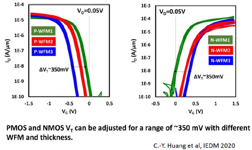
Experimental data illustrating the range of multiple Vt device characteristics for monolithic nFETs and pFETs is shown below.
Although CFET device technology promises continued improvements in PPA over the upcoming nanoribbon process nodes, a key consideration will be the ultimate cost of the CFET device topology. Marko presented the following cost estimate comparisons, part of a collaboration with IC Knowledge LLC. The category breakdowns are: lithography, deposition, etch, CMP, metrology, and other. Note that the CFET examples include a BPR distribution, opening up additional cell tracks for signal routing. The major contributors to the sequential CFET cost difference are the wafer bonding and separate top device processing.
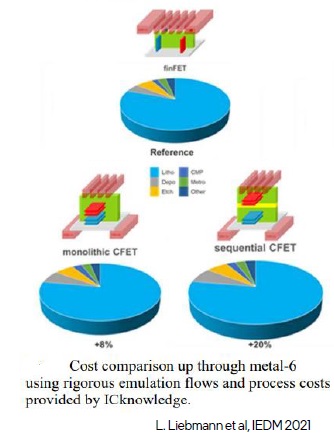
In total, the PPAC benefits of CFET fabrication look compelling, over though the total CFET process cost is higher. (A more challenging tradeoff is whether the flexibility afforded by sequential CFET device fabrication with different substrates will warrant the additional cost.)
Summary
Although process development challenges remain to be solved, a CFET device process roadmap appears to be a natural extension to the nanoribbon devices soon to achieve production status.
At the recent VLSI Symposium on Technology and Circuits, Intel presented both their R&D results and experimental data from other researchers demonstrating a compelling PPAC benefit. The longevity of FinFET devices will have lasted a little more than a decade through seven process node generations, as depicted below.
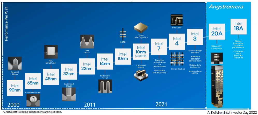
To date, roadmaps for nanoribbon devices depict (at least) two nodes.
The benefits of CFET devices and the leverage of nanoribbon fabrication (and modeling and EDA infrastructure) expertise may result in a shorter longevity for nanoribbons.
-chipguy
Also Read:
Intel Foundry Services Puts PDKs in the Cloud
An Update on In-Line Wafer Inspection Technology
Share this post via:


Comments
There are no comments yet.
You must register or log in to view/post comments.