You are currently viewing SemiWiki as a guest which gives you limited access to the site. To view blog comments and experience other SemiWiki features you must be a registered member. Registration is fast, simple, and absolutely free so please,
join our community today!
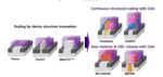
The transition from FinFET to Gate-All-Around (GAA) transistor technology represents a pivotal moment in the evolution of logic devices, driven by both physical scaling limits and the rapidly growing computational demands of artificial intelligence. As semiconductor technology approaches the sub-3 nm regime, traditional… Read More
In the early 2000s, Moore’s Law—the observation that the number of transistors on a chip doubles roughly every two years—was facing an existential crisis. As semiconductor nodes shrank below 90nm, planar transistors suffered from debilitating issues: leakage currents soared, power efficiency plummeted, and scaling became… Read More
Alchip Technologies Ltd., a global leader in high-performance computing (HPC) and artificial intelligence (AI) ASIC design and production services, continues its trajectory of rapid growth and technical leadership by pushing the boundaries of advanced-node silicon, expanding its global design capabilities, and building… Read More
IEDM turned 70 last week. This was cause for much celebration in the form of special events. One such event was a special invited paper on Tuesday afternoon from Intel’s Tahir Ghani, or Mr. Transistor as he is known. Tahir has been driving innovation at Intel for a very long time. He is an eyewitness to the incredible impact of the Moore’s… Read More
The world is abuzz with 3nm and 2nm technology availability. These processes offer the opportunity to pack far more on a single die than ever before. The complex digital systems contemplated will bring new AI algorithms to life and much more. But there is another side of the technology migration story. With all that digital processing… Read More
The VLSI Symposium on Technology and Circuits provides a deep dive on recent technical advances, as well as a view into the research efforts that will be transitioning to production in the near future. In a short course presentation at the Symposium, Marko Radosavljevic, from the Components Research group at Intel, provided … Read More
Introduction
Intel recently provided a detailed silicon process and advanced packaging technology roadmap presentation, entitled “Intel Accelerated”. The roadmap timeline extended out to 2024, with discussions of Intel client, data center, and GPU product releases, and especially, the underlying technologies to be … Read More
The annual VLSI Symposium provides unique insights into R&D innovations in both circuits and technology. Indeed, the papers presented are divided into two main tracks – Circuits and Technology. In addition, the symposium offers workshops, forums, and short courses, providing a breadth of additional information.
At… Read More
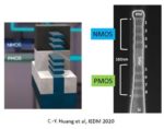
The next transition from current FinFET devices at advanced process nodes is the “nanosheet” device, as depicted in the figure below. [1]
The FinFET provides improved gate-to-channel electrostatic control compared to a planar device, where the gate traverses three sides of the fin. The “gate-all-around” characteristics… Read More
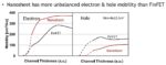
As transistor dimensions shrink to follow Moore’s Law, the functionality of the gate used to switch on or off the current is actually being degraded by the short channel effect (SCE) [1-5]. Moreover, the simultaneous reduction of voltage aggravates the degradation, as will be discussed below.
A Practical Lower Limit of… Read More