You are currently viewing SemiWiki as a guest which gives you limited access to the site. To view blog comments and experience other SemiWiki features you must be a registered member. Registration is fast, simple, and absolutely free so please,
join our community today!
WP_Term Object
(
    [term_id] => 16126
    [name] => Lithography
    [slug] => lithography
    [term_group] => 0
    [term_taxonomy_id] => 16126
    [taxonomy] => category
    [description] =>
    [parent] => 0
    [count] => 187
    [filter] => raw
    [cat_ID] => 16126
    [category_count] => 187
    [category_description] =>
    [cat_name] => Lithography
    [category_nicename] => lithography
    [category_parent] => 0
    [is_post] =>
)
In the pursuit of advanced extreme ultraviolet (EUV) lithography for high-NA patterning, metal oxide resists (MORs) offer significant promise but face challenges like critical dimension (CD) variation due to atmospheric interactions. Presented at SPIE Advanced Lithography + Patterning 2025 by Kevin M. Dorney and colleagues… Read More
The imec installation of the ASML EXE:5200 High Numerical Aperture (High NA) extreme ultraviolet (EUV) lithography system at imec represents a pivotal advancement in semiconductor manufacturing and research. This system, installed in imec’s 300 mm cleanroom in Leuven, Belgium, introduces unprecedented lithographic resolution… Read More
As semiconductor manufacturing pushes deeper into the nanometer regime, computational lithography has evolved from a supporting step into a central pillar of advanced chip design. Mask synthesis, lithography simulation, and optical proximity correction (OPC) now demand unprecedented levels of accuracy and computational… Read More
In the realm of extreme ultraviolet (EUV) lithography, metal oxide resists (MORs) have emerged as promising candidates for advanced semiconductor patterning. However, their stability poses challenges, particularly interactions with clean-room environments like humidity and airborne molecular contaminants (AMCs) … Read More
In the modern world, the semiconductor industry stands at the heart of technological innovation. From smartphones and laptops to advanced medical devices and artificial intelligence systems, nearly every piece of contemporary electronics depends on increasingly sophisticated microchips. Among the leading companies … Read More
With over 25 years of experience in the specialty materials industry, Dr. Heinz Kaiser is a member of the Management Board of SCHOTT AG, responsible for High-Performance Materials and Flat Glass, while also heading Sales and Market Development, Sales Excellence, and Intellectual Property. With a strong engineering background… Read More
Earlier this month, TechInsights did a teardown of the Kirin 9030 chip found in Huawei’s Mate 80 Pro Max [1]. Two clear statements were made on the findings: (1) the transistor density of SMIC’s “N+3” process was definitely below that of the earlier 5nm processes from Samsung and TSMC, and (2) metal pitch was aggressively scaled
…
Read More
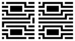
The patterning of features outside a DRAM cell array can be just as challenging as those within the array itself [1]. The array contains features which are densely packed, but regularly arranged. On the other hand, outside the array, the minimum pitch features, such as the lowest metal lines in the periphery for the sense amplifier… Read More
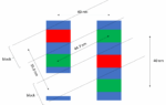
For the so-called “2nm” node or beyond, the minimum metal pitch is expected to be 20 nm or even less, while at the same time, contacted gate pitch is being pushed to 40 nm [1]. Therefore, we expect via connections that can possibly be as narrow as 10 nm (Figure 1)! For this reason, it is natural to expect High-NA EUV lithography as the go-to
…
Read More
While stochastic defects link yield with the practical resolution of EUV lithography resulting from its quantum nature [1], very low yields of EUV processes are more readily linked to the use of EUV masks without pellicles. Pellicles are thin film membrane covers on masks (regardless of wavelength: EUV and DUV and i-line) used… Read More


Is Intel About to Take Flight?