You are currently viewing SemiWiki as a guest which gives you limited access to the site. To view blog comments and experience other SemiWiki features you must be a registered member. Registration is fast, simple, and absolutely free so please,
join our community today!
WP_Term Object
(
    [term_id] => 158
    [name] => Foundries
    [slug] => semiconductor-manufacturers
    [term_group] => 0
    [term_taxonomy_id] => 158
    [taxonomy] => category
    [description] =>
    [parent] => 0
    [count] => 1368
    [filter] => raw
    [cat_ID] => 158
    [category_count] => 1368
    [category_description] =>
    [cat_name] => Foundries
    [category_nicename] => semiconductor-manufacturers
    [category_parent] => 0
    [is_post] =>
)
The opening of the TSMC 2026 earning call series brought no surprises. CC Wei has done more than 30 such calls since taking the CEO position in 2018 and he never fails to disappoint. Once again, CC Wei reported numbers above guidance driven by strong demand and flawless execution. This illustrates the benefit of TSMC’s close collaborations… Read More
Everyone has been treating Intel as a turnaround story. What if it’s not a scheduled airline — but a charter, and Musk is the one filing the flight plan? Not just Tesla. Companies like Microsoft, Google, Meta, and Oracle are all designing their own silicon now, and their AI infrastructure depends on it. And yet they remain dependent… Read More
Intel, Musk, and the Tweet That Launched a 1000 Ships on a Becalmed Sea
Why do professional executives running major corporations frame a major moment in their company’s history with a tweet? Jerry Sanders spent his career yelling “real men have fabs!” Now Intel has fabs–and apparently tweets about … Read More
Agentic AI workloads are reshaping the compute requirements of modern data center infrastructure by shifting performance bottlenecks from GPU-centric inference to CPU-heavy orchestration and workflow management. Traditional AI inference pipelines relied primarily on GPUs performing a single forward pass, where input… Read More
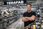
At the TERAFAB launch event in Austin on March 21, Elon Musk made a prediction that would have sounded like science fiction a decade ago—and may still: roughly 80 percent of AI compute will eventually move off-planet.
The argument is straightforward once you accept his premises. Earth-based data centers face three hard constraints—land,… Read More
As semiconductor technology advances into increasingly complex and expensive process nodes, the economic and technical risks associated with ASIC design have grown dramatically. At advanced nodes such as Intel 18A, the cost of a single design error can escalate into tens of millions of dollars, compounded by months of delay.… Read More
Intel has posted three consecutive years of falling revenue and an $18.76 billion loss in 2024 alone—and the U.S. government has handed it tens of billions of dollars to fix the problem. The government money isn’t fixing the real issue, which isn’t technical. It’s cultural. Intel got slow, political, and risk-averse—the… Read More
One of my favorite times of the year is coming (sailing season) and my favorite event of the year is coming as the company I most respect will host the best international semiconductor networking event starting here in Silicon Valley.
The 32nd annual TSMC Technology Symposium represents one of the most influential events in the … Read More
The majority of my 40+ year career has been spent managing the relationship between leading-edge semiconductor design and manufacture, working with just about every commercial foundry and top customer in one way or another. It’s my thing—it fascinates me. I’m also a fan of disruption, and the latest disruptions the semiconductor… Read More
How do you get a shortage while not growing???
Intel Announced earnings in January. Then David Zinsner presented updates on business this week. David is open when talking and always shares 2-3 things he probably should not share. Often he shares things some of us know, but we cannot present because it is not public. Then he makes it… Read More


Intel, Musk, and the Tweet That Launched a 1000 Ships on a Becalmed Sea