Introduction
Intel recently provided a detailed silicon process and advanced packaging technology roadmap presentation, entitled “Intel Accelerated”. The roadmap timeline extended out to 2024, with discussions of Intel client, data center, and GPU product releases, and especially, the underlying technologies to be incorporated into those products.
This article will focus on the technology roadmaps, rather than the “Lake” (client) and “Rapids” (data center) product families, such as Meteor Lake, Sapphire Rapids, and Granite Rapids. Also, look for an upcoming article on how the Intel Foundry Services (IFS) initiative will also be leveraging these technology introductions.
Scott Jones published a comprehensive SemiWiki article summarizing the revised silicon process nomenclature that Intel will be adopting – link.
Personally, of all the criteria used to evaluate a silicon process for a potential product design – e.g., performance per watt, circuit/SRAM density, IP availability, low power options, cost, qualification at environmental corners, lifetime reliability – the actual process node name is not one of them. Nevertheless, Intel has updated their process nomenclature to “sorta” align with other foundry naming conventions. The timeline for these process node introductions is discussed next.
5 Nodes in 4 Years
Pat Gelsinger, Intel CEO, described the process technology (and Intel CPU) roadmap in the following manner, “We will continue the model of micro-architecture development and process introduction, but at a torrid pace. The spirit of the Tick-Tock release model is alive, but with focus on more parallel innovation. We will de-risk new technology introductions. Proven micro-architectures will be transitioned to new process nodes. As an example, the upcoming backside power distribution technology will be proven using the I3 technology node before introducing into high volume manufacturing with the I20A node. Also, the requisite capital equipment and staffing requirements for this roadmap are fully funded.”
Note that the process descriptions that were provided focused on “performance per watt” (more on that later), as opposed to circuit density scaling. Here is the silicon process roadmap:

10 SuperFin (10SF)
- currently in volume production,
- “the most significant intra-node performance improvement (over 10+) in Intel’s history”
I7 (was originally denoted as “10 Enhanced SuperFin”)
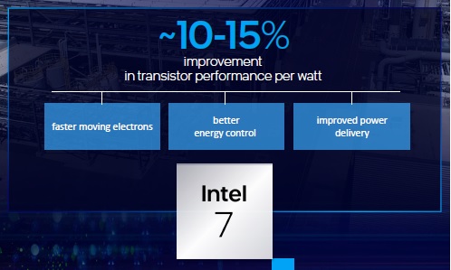
- +10-15% performance per watt gains over 10SF
- increased device channel strain
- Alder Lake (big/little X86 core mix) available late 2021, Sapphire Rapids available 1Q22
I4
- +20% performance per watt improvement over I7
- first introduction of EUV lithography
- ramp in 2H22, high volume manufacturing in 2023 (Meteor Lake, Granite Rapids)
I3
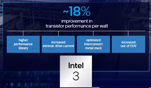
- +18% performance per watt compared to I4 (FinFET-based)
- new high-performance library
- improved transistor drive current
- improved BEOL characteristics (e.g., reduced via resistance)
- increased EUV deployment
- ramp in 2H2023, HVM in 2024
I20A
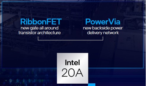
- ramp in 1H2024
- transition to “ribbon FET” (gate-all-around) device topology
- introduction of backside power delivery
I18A
- ramp in 1H2025
Although there is some flexibility in the definition of process introduction “ramp” compared to high volume manufacturing, the timeline for this roadmap is indeed extremely aggressive.
As mentioned above, the focus of the process roadmap discussion was to highlight the performance-per-watt comparisons between nodes.
I had the opportunity to chat briefly with Sanjay Natarajan, Senior VP and co-General Manager for Logic Technology Development, who indicated, “We have the line of sight in place to realize this process roadmap.” I asked Sanjay about the performance per watt improvement targets. He replied, “This is a result of a comprehensive analysis across a broad suite of designs – from ring oscillators and cell libraries to large building blocks and cores in a product-like environment. These improvements are from many process optimizations – not just transistor drive current, but also throughout the interconnect stack, including power delivery.”
EUV
Intel has been conservative in their deployment of (0.33NA) extreme ultra-violet lithography, and their assessment of the cost/yield tradeoffs between EUV and DUV multipatterning litho.
As described above (and summarized in Scott’s article), process node I4 will be the first to incorporate (limited) EUV mask layers in 2H2022, with greater adoption in node I3 (2H2023).
Dr. Ann Kelleher, Senior VP and General Manager, Technology Development, highlighted, “The four pillars of EUV lithography have achieved manufacturing maturity – photoresist, masks, pellicles, and metrology.”
Ann also mentioned that Intel anticipates being the first to incorporate (0.55NA) “high NA” EUV lithography (for the I18A node), as a result of their collaboration with ASML. (For more info on the challenges of high NA EUV photoresist development, here is an earlier SemiWiki article from Intel R&D – link.)
GAA
As mentioned above, node I20A incorporates a transition from FinFET devices to a gate-all-around configuration, denoted by Intel as “ribbon FETs”, illustrated below.
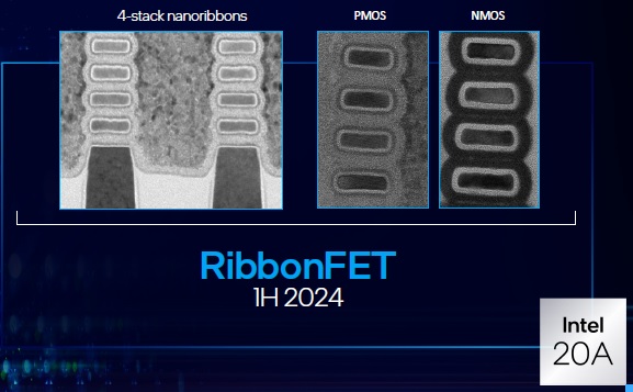
(A cynical engineer would observe that there are several different names being used for the GAA device – so much for nomenclature consolidation in the industry.)
The figure above shows 4 stacked device channels surrounded by the gate – clearly, a performance-oriented implementation. Researchers are actively evaluating the “optimum” number of stacked channels, as well as the minimum/maximum channel width design flexibility; there is also active research to evaluate the process complexity and yield impact of locally removing channel(s) from the stack for circuit applications that would leverage lower device drive current (at minimum width).
Backside Power Delivery and “Power Vias”
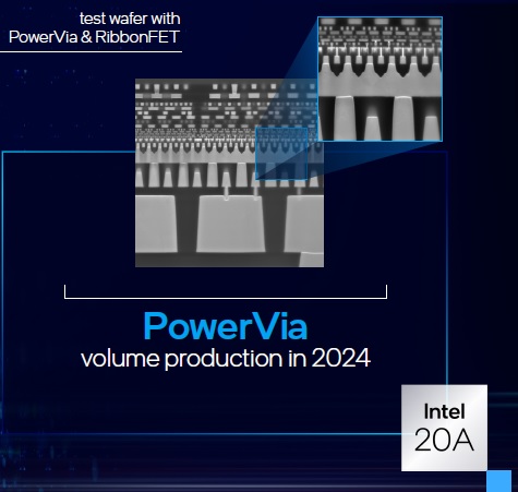
Intel showed die cross-sections of backside power delivery metallization, utilizing “power vias” – the target node is I20A, concurrent with the ribbon FET introduction.
Sanjay indicated, “There are significant benefits to both improved signal routing track availability and reduced power distribution network losses with backside power delivery. There are challenges, as well, working with the thinned wafer substrate. We have broad expertise across both silicon and packaging technology development groups, for the requisite grinding, etch, and fill steps.”
Sanjay added, “The power via strategy provides full connectivity to the circuitry fundamental to power state management of the PDN.”
IDM 2.0 and IFS
Pat G. also clarified the company strategy with regards to the Integrated Device Manufacture (IDM2.0) business model, and the renewed emphasis on providing foundry services.
- “We will continue to manufacture the majority of our products internally, with some outsourcing. We are making considerable investments in expanding and updating fabs in Oregon, Arizona, and Israel (silicon), as well as in New Mexico (advanced packaging).”
- “These advanced process nodes will be available to IFS customers.” (Intel announced an IFS collaboration with Qualcomm, focused on the I20A node.)
Packaging Roadmap
Intel’s advanced packaging investments will continue evolutionary enhancements to their 2.5D and 3D offering, to optimize multi-die integration and die interface bandwidth.
EMIB
The Embedded Multi-die Interconnect Bridge (EMIB) provides for 2.5D package interconnections between die, introduced by Intel in 2017. it utilizes a dense pitch microbump connection between the die edges and a silicon “bridge”, as shown below. (also, a previous SemiWiki article link)
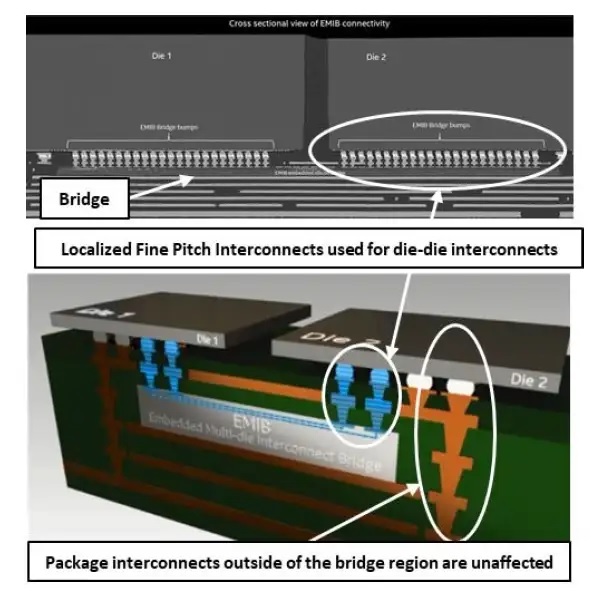
There is a significant cost benefit compared to a full-size silicon interposer, especially considering the increased number of die (and die stacks) integrated into the final package, which requires >1X maximum silicon lithography reticle size. As an example, Sapphire Rapids will be a 92mm x 92mm BGA package. (Wow.)
The EMIB microbump pitch roadmap depicts a transition from 55um to 45um (used on Sapphire Rapids) to 40um.
Foveros
Intel’s 3D stacked die technology is denoted as Foveros. As illustrated in the figures below, Foveros encompasses two configurations – a microbump-based die attach technology, and a direct hybrid bonded connection.
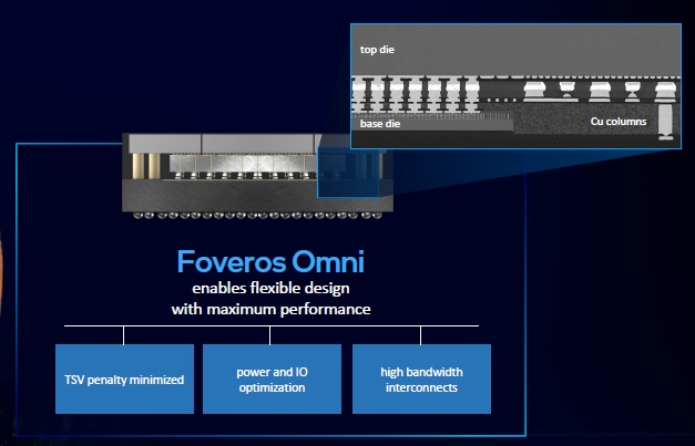
The second generation microbump Foveros technology, denoted as Foveros-Omni, introduces a 36um microbump pitch. The upcoming Meteor Lake product family announcement in process node I4 will showcase the Foveros-Omni offering.
The roadmap presented suggests a subsequent microbump pitch of 25um. Through silicon vias and through package copper columns complete the overall package interconnect offering.
Pat G. indicated, “Foveros-Omni offers an attractive cost-performance-power benefit (compared to EMIB) for client products in the mobile markets.”
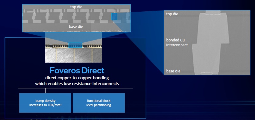
Foveros-Direct is the hybrid bonded package designation, to be released in 2023.
I had a chance to chat briefly with Dr. Babak Sabi, VP and General Manager of the Assembly and Test Technology Development group, about the EMIB and Foveros packaging strategy. He indicated, “The Foveros-Direct introduction will utilize a ‘sub-10um’ hybrid bond pitch, offering an exceptional die-to-die connectivity density. (~10K/mm**2) Our assembly and test technology team is implementing improved die sort technologies for the known-good die integrated into these packages.”
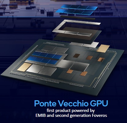
Babak added, “Further, the EMIB and Foveros technologies are complementary. An example of a combined EMIB and Foveros implementation is the upcoming Ponte Vecchio GPU.”
I asked Babak about some of the challenges in the development of these packaging technologies. He replied, “For Foveros-Omni, mechanical alignment of the stacked die is a challenge, especially as we look to scale the bump pitch below 25um, to the 15-20um range. Another big issue is to have clean die edges after separation – you need to have no particulates introduced during the assembly process. And, we are working closely with EDA tool providers on signal integrity and power distribution network modeling and simulation, and especially on the thermal-mechanical analysis of the entire assembly. These complex packages need to be correct-by-construction.”
Futures
- Intel’s Innovation Event will be a (hybrid) conference in San Francisco on October 27-28 (likely including the Alder Lake client CPU announcement).
- According to Pat G., expect an announcement on fab expansion “by year end”. (This was mentioned in the context of Intel’s support for US and EU government support for increased domestic fabrication.)
- Process node I18A was mentioned briefly, targeting initial availability in 1H2025.
- Intel has been investing significantly in (integrated) silicon photonics circuitry, for optimized interface bandwidth and “picoJoules per bit” power dissipation.
Summary
Intel has clearly re-focused their considerable expertise in materials, lithography, and device technologies. They have presented an aggressive silicon and packaging technology roadmap – especially noteworthy is the cadence of new process introductions (and, significantly, to offer these technologies to IFS customers, as well).
As far as the execution of this roadmap, Sanjay’s quote of confidence is especially noteworthy, “We have line-of-sight into these innovations.”
(Personally, I’ll reserve judgment on the high NA EUV rollout, but that’s not expected until 2025.)
Interesting times, indeed.
-chipguy
Share this post via:


Comments
3 Replies to “Highlights of the “Intel Accelerated” Roadmap Presentation”
You must register or log in to view/post comments.