The evolution of low-cost heterogeneous multi-chip packaging (MCP) has led to significant system-level product innovations. Three classes of MCP offerings have emerged:
- wafer-level fan-out redistribution, using reconstituted wafer substrates of molding compound as the surface for interconnections between die (2D)
- a separate silicon-based interconnect layer for redistribution, either a full-sized silicon interposer or die-to-die silicon bridges embedded in the organic package (2.5D)
- face-to-face or face-to-back die stacked vertically, utilizing hybrid bonding of die pads, with through-die vias (3D)
The 2.5D solution has received considerable R&D investment, to support larger package sizes and greater interconnect redistribution density (i.e., line + space pitch, number of metal layers). The integration of multiple, smaller die provides chip and package assembly yield and cost tradeoffs.
The functionality integrated in the 2.5D MCP has become increasingly diverse – e.g., CPUs, GPUs, memory (especially HBM stacks), FPGAs, network switches, I/O transceivers, hardware accelerators for specific applications. Current R&D efforts will continue to extend the breadth of this system-in-package composition – the next “big thing” could likely be the integration of optoelectronic conversion elements, enabling the efficiencies of photonic-based data transfer over medium- and short-range lanes.
A key facet to enabling the growth of 2.5D MCP offerings is the technology for the internal connectivity between die in the package. As mentioned above, one alternative is to fabricate the wires on a silicon interposer, whose dimensions equate to the full package size. Recent advances have enabled interposers to exceed the 1X maximum reticle size for die placement and interconnect. Another is to fabricate a small silicon bridge for the wires, embedded in an organic package, spanning the edges of adjacent die.
Intel’s Embedded Multi-Die Interconnect Bridge (EMIB) is an example of 2.5D MCP bridge interconnect technology. It has been briefly described in previous SemiWiki articles (link).
With the recent re-introduction of Intel Foundry Services, I thought it would be appropriate to dive a bit more deeply into this technology, as it will no doubt be a fundamental part of ICF customer system implementations.
I had the opportunity to learn more about EMIB capabilities and potentials, in a most enlightening discussion with Ravi Mahajan, Intel Fellow in Assembly and Test Technology Development. This article summarizes the highlights of our discussion.
EMIB Fabrication
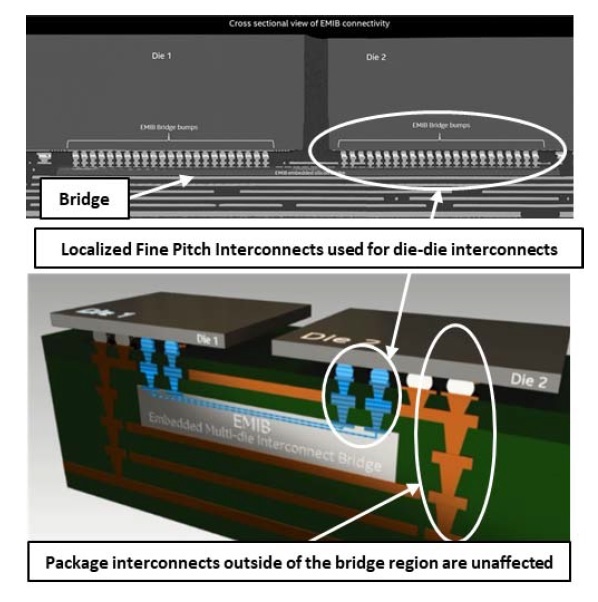
The figure above illustrates a cross-section of a typical EMIB bridge resident in the organic package. The bridge silicon resides in a package cavity, fabricated as depicted in the figure below. The top package metal layer provides a reference plane, with vias through the plane connecting the die and bridge.

Ravi indicated, “The EMIB process is built upon the standard package construction flow, with the additional steps to create the EMIB cavities. The bridges are positioned in the cavities, held in place with an adhesive. The final dielectric and metal build-up layers are added followed by via drilling and plating.”
Note in the cross-section picture above the reference to coarse and fine vias, corresponding to the two different bump pitches present on each die, as shown below.
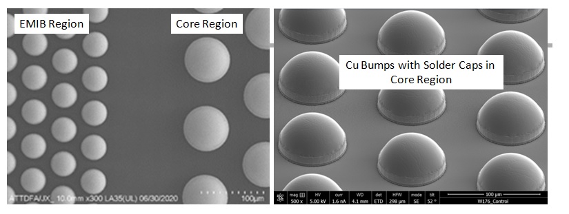
The coarse bumps are used for die-to-package trace layer connections, while the fine pitch is associated with the EMIB connections – more on the target EMIB connection density shortly.
Ravi added, “Considerable engineering effort was invested to define the fine and coarse bump profiles that would support die attach and via connection processing. Specifically, that included focusing on bump height control and solder volume. We have worked with bumping providers to enable this dual pitch and profile configuration. In addition, each die in the MCP package is attached individually – the bumps on the die will be subjected to multiple reflow cycles. Attention was paid to the flux materials incorporated with the bumps. A process to provide void-free epoxy underfill throughout the bump regions has also been developed. The materials, bumps, and the attach process are all in high volume manufacturing.”
EMIB Physical Implementation
An example of a fabricated bridge is shown below. This specific design implements the following:
- 55um bump pitch to the die above
- 2um line + 2um space, with 2um metal thickness
- 4um pitch, with 250 wires per mm “beachfront”
- 2um thick dielectric between each EMIB metal layer
- 4 metal layers on the EMIB bridge, M1 and M3 are dedicated to GND planes
- signal layers that typically utilize a 3 signal + 1 ground shield pattern on M2 and M4
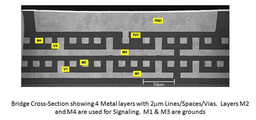
To be precise, the metal planes on the alternate EMIB layers are implemented as a mesh, as depicted below.
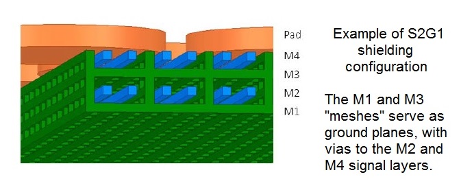
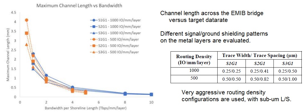
Ravi said, “The design of the EMIB interconnects is an intricate tradeoff between multiple targets – the interconnect density (wires per die edge per mm, bumps per mm**2), power constraints, and signaling bandwidth. For each die, that implies driver sizing and receiver sensitivity. For power savings, an unterminated receiver is typically used (i.e., capacitive load only, no resistive termination). To address those targets, the EMIB design considerations include line and space dimensions, bump pitch, channel length, metal thickness, and dielectric material between the metal layers. The design of the electrical signal shielding (e.g., S1G1, S2G1, S3G1) is also crucial.”
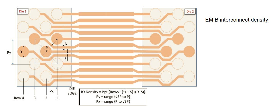
The figure below shows the layout view of the interconnect density design, including how the bridge signals reach multiple rows of fine-pitch bumps on adjacent die. The table below illustrates the range of dimensions and pitches available.

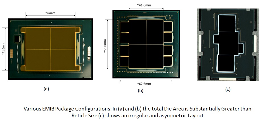
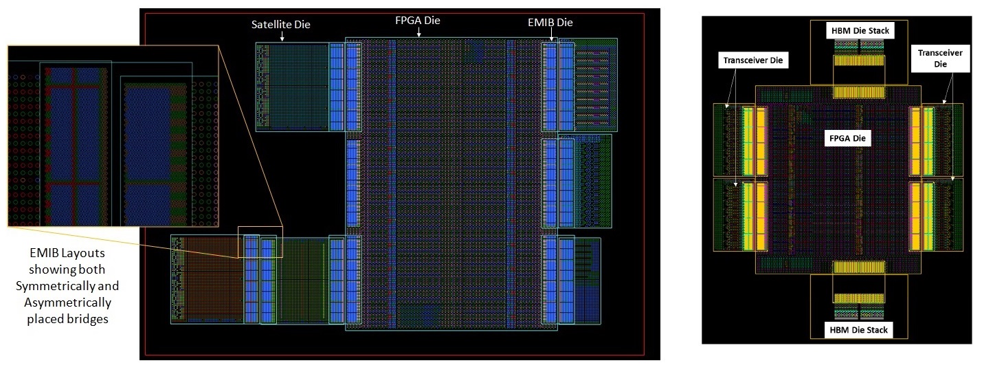
The figures below show various bridge positioning options. Note that there is considerable flexibility in bridge placement – e.g., horizontal and vertical orientations, asymmetric locations relative to die edges.
EMIB Electrical Characteristics
Intel has published a detailed electrical analysis for the EMIB interconnect, evaluating insertion loss and crosstalk for various signal-ground shielding combinations and wire lengths. (References appended at the end of this article.)
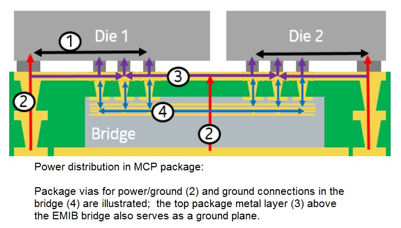
The figure above highlights the power distribution paths in the package. Note that the small footprint of the EMIB bridge means the balance of the I/O signal and power integrity characteristics are unaffected, unlike a full silicon interposer where all signal and power vias must first traverse through the interposer. As mentioned earlier, the top package layer above the EMIB serves as a ground plane, as well.
The figure below shows an example of the electrical analysis results, depicting the maximum EMIB signal length for a target cumulative beachfront bandwidth for various signal shielding patterns. Aggressive L/S wire pitch designs were assumed for this example. The electrical model used:
- a simple output driver (R=50ohms, C=0.5pF)
- an unterminated receiver (C=0.5pF)
- four-layer EMIB metal stack-up, dielectric constant=4.0
- top package metal plane above the embedded bridge
- a 1V signal swing with a 200mV vertical eye opening receiver sensitivity (incorporating the near-end and far-end crosstalk for the unterminated, capacitive receiver)
EMIB Design Services
Due to the intricacies of the EMIB design tradeoffs, Ravi indicated, “Intel will collaborate closely with the foundry customers on their product requirement, and develop the EMIB designs as a service. We will work with the customers on die pinout and bump patterns, and provide the EMIB silicon implementations that address their datarate targets.”
EMIB Future Development
EMIB technology continues to be an R&D focus at Intel. Ravi highlighted, “We will continue to work on providing greater interconnect edge density, including tighter bump pitch and more aggressive line/space EMIB metal pitch (sub-1um). It’s certainly feasible to incorporate active circuitry into the EMIB, as well.”
Summary
The EMIB bridge approach in support of advanced MCP technology offers some unique advantages:
- extension of existing organic packaging technology
- enables large die count and large package configurations
- lower cost than a full-size silicon interposer
- support for high datarate signaling between adjacent die, using simple driver/receiver circuitry
- ability to optimize each die-die link individually by customizing the bridge for that link
The EMIB links are power-efficient, with low metal R*C delays, with minimal latency and high signal integrity.
There are some EMIB disadvantages, which have been addressed by the Intel R&D team:
- additional complexity in the die bumping and package assembly process
- disparate coefficient-of-thermal-expansion (CTE) factors between the package, the die, and the EMIB bridge
The EMIB silicon is thinned prior to package assembly (t < 75um), and thus doesn’t significantly alter the thermally-induced mechanical strain between package and die and the bumps plus underfill interface. The overall reliability is comparable to a conventional organic package.
The support provided by the packaging team at the Intel Foundry Services will assist customers seeking advanced MCP solutions to achieve their signaling datarate, power, and cost targets.
The growth of MCP packaging adoption will no doubt continue to accelerate. (The DARPA CHIPS program will also contribute to greater interest in MCP design.)
For more information on Intel’s EMIB offerings, please follow this link, and be sure to consult the references below.
-chipguy
References
[1] Mahajan, R., et al., “Embedded Multi-Die Interconnect Bridge (EMIB) – A High Density High Bandwidth Packaging Interconnect”, 2016 IEEE 66th ECTC conference, p. 557-565.
[2] Durgun, A., et al., “Electrical Performance Limits of Fine Pitch Interconnects for Heterogeneous Integration”, 2019 IEEE 69th ECTC conference, p. 667-673.
[3] Mahajan, R., et al., “Embedded Multidie Interconnect Bridge – A Localized, High-Density Multichip Packaging Interconnect”, IEEE Transactions on Components, Packaging, and Manufacturing Technology, Vol. 9, No. 10, October, 2019, p. 1952-1962.
Share this post via:


Comments
One Reply to “Intel’s EMIB Packaging Technology – A Deep Dive”
You must register or log in to view/post comments.