You are currently viewing SemiWiki as a guest which gives you limited access to the site. To view blog comments and experience other SemiWiki features you must be a registered member. Registration is fast, simple, and absolutely free so please,
join our community today!
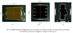
The evolution of low-cost heterogeneous multi-chip packaging (MCP) has led to significant system-level product innovations. Three classes of MCP offerings have emerged:
- wafer-level fan-out redistribution, using reconstituted wafer substrates of molding compound as the surface for interconnections between die (2D)
…
Read More
Summary
Thermo-compression bonding is used in heterogeneous 3D packaging technology – this attach method was applied to the assembly of large (12-stack and 16-stack) high bandwidth memory (HBM) die, with significant bandwidth and power improvements over traditional microbump attach.
Introduction
The rapid growth of heterogeneous… Read More
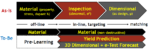
There have been a multitude of announcements recently relative to the incorporation of machine learning (ML) methods into EDA tool algorithms, mostly in the physical implementation flows. For example, deterministic ML-based decision algorithms applied to cell placement and signal interconnect routing promise to expedite… Read More
Summary
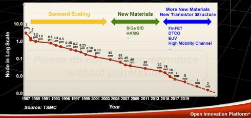
Design Technology Co-Optimization (DTCO) analysis was pursued for library cell PPA estimates for gate-all-around (GAA) devices and new metallurgy options. The cell design and process recommendations are a bit surprising.
Introduction
During the “golden years” of silicon technology evolution that applied Dennard… Read More
Daniel Nenni was gracious enough to encourage me to conduct a brief webinar describing a new reference text, recently published by Prentice-Hall, part of the Semiwiki Webinar Series.
VLSI DESIGN Methodology Development Webiner Replay
Background
I was motivated to write the text to provide college students with a broad background… Read More
The recent Design Automation Conference in Las Vegas was an indication of how the electronics industry is evolving. In its formative years, DAC was focused on the fundamental algorithms emerging from academic research and industrial R&D, that enabled the continuation of the Moore’s Law complexity curve. (Indeed, the… Read More
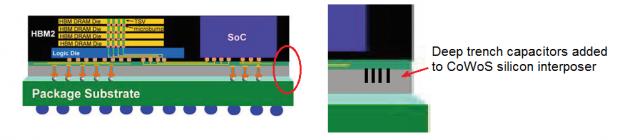
TSMC recently held their annual Technology Symposium in Santa Clara. Part 1 of this article focused on the semiconductor process highlights. This part reviews the advanced packaging technologies presented at the symposium.
TSMC has clearly made a transition from a “pure” wafer-level foundry to a supplier of complex integrated… Read More
Each year, TSMC conducts two major customer events worldwide – the TSMC Technology Symposium in the Spring and the TSMC Open Innovation Platform Ecosystem Forum in the Fall. The Technology Symposium event was recently held in Santa Clara, CA, providing an extensive update on the status of advanced semiconductor and packaging… Read More
This year TSMC did a FinFET victory lap with the success of 16nm, 12nm, 10nm, and 7nm. It really is well deserved. Even though TSMC credits the ecosystem and customers, I credit TSMC and their relationship with Apple since it has pushed us all much harder than ever before. TSMC CEO C.C. Wei summed it up nicely in his keynote: Innovation,… Read More
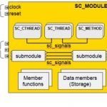
Update on SystemC for High-Level Synthesisby Tom Dillinger on 03-26-2019 at 12:00 amCategories: Cadence, EDA
The scope of current system designs continues to present challenges to verification and implementation engineering teams. The algorithmic complexity of image/voice processing applications needs a high-level language description for efficient representation. The development and testing of embedded firmware routines… Read More