
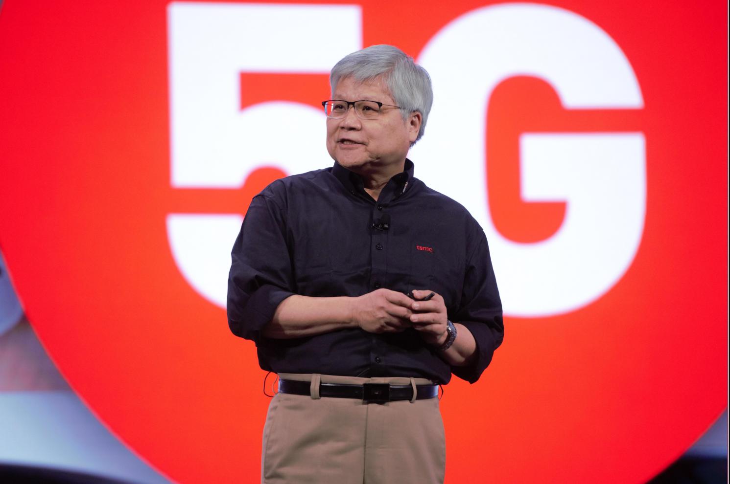
 This year TSMC did a FinFET victory lap with the success of 16nm, 12nm, 10nm, and 7nm. It really is well deserved. Even though TSMC credits the ecosystem and customers, I credit TSMC and their relationship with Apple since it has pushed us all much harder than ever before. TSMC CEO C.C. Wei summed it up nicely in his keynote: Innovation, collaboration, and hard work.
Tom Dillinger also attended and he will be writing in more detail next week. Tom has been busy of late. He just finished his second textbook on VLSI Design Methodology Development for Prentice Hall. Remember, Tom started the FinFET discussion on SemiWiki in 2012 so you can bet FinFETs will be mentioned a time or two.
Here is an outline of what Tom will be writing about next week so stay tuned:
Advanced Technology Development and Materials Engineering:
1) N7/N7+ update
highlights: “Making 5G a Reality” — N7 as a technology enabler; D0 defect density improvement; 112Gbps PAM4 SerDes IP
2) N6 update
highlights: PPA comparisons to N7; ease of RTO/NTO migration from N7; new M0 routing (very unique!)
3) N5 update
highlights: schedule; D0 ramp; PPA comparisons to N7; “designed from the start for both mobile and HPC platforms”
4) Advanced process development / materials engineering
highlights: additional Vt devices for HPC in N5 and ULL/ULP technologies; high mobility (Ge) channel device; metal RIE (replacing damascene patterning); new metallization materials (graphene cap on Cu); future research into 2D semiconductor materials
5) Manufacturing excellence
highlights: focus on in-line process monitoring; maverick lot identification; “ink out good die in a bad zone” (very unique!); Continuous Process Improvement focused on wafer edge (very unique!); product-specific UpperSpecLimit + LowerSpecLimit statistical process control (also very unique!)
6) Roadmap for automotive platform
highlights: new “L2+” automotive grade introduced; focus on DPPM reduction; MCU’s in a vehicle transitioning from eFlash to MRAM memory offering
7) Roadmap for IoT platform
highlights: new eHVT device; unique analog device process engineering; new “dual-rail VDD” SRAM offerings (aggressive SRAM_Vmin scaling); MRAM roadmap
8) RF process development focus
highlights: device engineering to improve ft and fmax (in several processes), new thick metal to improve inductor Q factor; device model characterization
Although the specialty technologies presentation was very interesting, there’s probably not enough room in the article to cover MEMS, CIS (at near infrared wavelengths), etc.
“Front-End” and “Back-End” Advanced Packaging:
1) SoIC
highlights: diverse die size and stacking options (e.g., face-to-face and face-to-back bonding)
2) CoWoS
highlights: reticle size roadmap, embedded deep trench caps (DTC) in Silicon interposer
3) InFO
highlights: InFO_PoP through InFO via (TIV) scaling; InFO without substrate (2020)
4) 3DIC ecosystem support
History is always a part of semiconductor symposiums because semiconductors really have come a long way fueled by a series of technological disruptions. When I went away to college my beautiful girlfriend (wife) used to write letters to me everyday and call me on the weekends. My parents and grandparents had similar experiences. Shortly after we married, PCs and the internet landed on our desks and we emailed and Usenet-ed our way around the world. Then came smartphones and social media, probably the biggest disruption of them all. Phones are now in our hands and faces more than ever before but that is going to change.
The next disruption will be fueled by 5G and AI which is just now beginning. If you think semiconductors are important today just wait another ten years because you will not be able to survive without them, absolutely.
TSMC and the semiconductor industry have been living a very mobile life since PCs and phones left our desks. Moving forward, AI enabled edge devices will continue to be a semiconductor industry driver but the real upside for the foundry business will be getting the many zettabytes of data into the cloud and processed. Today Intel CPUs and GPUs dominate the cloud. Tomorrow it will be custom AI processors built by the cloud companies themselves in close partnership with the fabless semiconductor ecosystem and that means TSMC.
From writing letters to “real-time thought processing” in one lifetime, simply amazing.
Also read: 2019 TSMC Technology Symposium Review Part I
Share this post via:


Comments
3 Replies to “A Quick TSMC 2019 Tech Symposium Overview”
You must register or log in to view/post comments.