You are currently viewing SemiWiki as a guest which gives you limited access to the site. To view blog comments and experience other SemiWiki features you must be a registered member. Registration is fast, simple, and absolutely free so please,
join our community today!
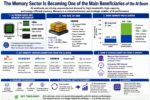
The explosive growth of artificial intelligence is transforming the semiconductor industry, and nowhere is this more evident than in the memory sector. AI training and inference workloads are fundamentally memory-intensive, driving unprecedented demand for advanced DRAM architectures, High Bandwidth Memory (HBM), and… Read More
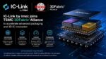
imec announced that IC-Link by imec has joined the TSMC 3DFabric Alliance, a strategically important move that reflects the semiconductor industry’s transition from traditional monolithic scaling toward heterogeneous integration, chiplet architectures, and advanced packaging-driven system optimization. The partnership… Read More
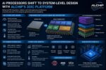
Artificial intelligence processors are entering a new era. For more than two decades, semiconductor innovation was driven primarily by transistor scaling and process node shrinks. Today, however, AI infrastructure demands are growing faster than traditional Moore’s Law improvements can sustain. The industry is now shifting… Read More
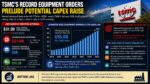
TSMC’s latest Board of Directors capital appropriation announcement may appear mixed on the surface, but a closer look reveals one important conclusion: The company is quietly setting the stage for another potential upward revision to its already aggressive 2026 capital expenditure outlook. The headline figure of $31.3B … Read More
A recent announcement from Synopsys signals a meaningful escalation in the race to build next-generation AI hardware. The expanded collaboration between Synopsys and TSMC brings together silicon-proven IP, AI-driven design tools, and cutting-edge manufacturing processes in a tightly integrated effort to accelerate high-performance… Read More
L.C. leads efforts in design enablement, ensuring that the company can meet the diverse and evolving requirements of its global customer base. Prior to this, he headed the Design and Technology Platform organization starting in 2018.
Since joining TSMC in 2000, Dr. Lu has held multiple leadership positions in design services.… Read More
The rapid rise of artificial intelligence is fundamentally reshaping computing architectures. As AI models scale toward trillions of parameters, traditional approaches to performance improvement are no longer sufficient. Instead, the industry is entering a new era where system-level innovation, advanced packaging, … Read More
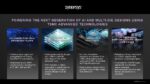
At its 2026 Technology Symposium, TSMC delivered a clear message: the AI era has entered a new phase. The primary constraint is no longer model capability, but the systems required to run those models at scale. Addressing this shift will demand significant advances in semiconductor technology, spanning compute, memory, interconnects,… Read More
Yes, it is that time of year again, the 2026 TSMC Technology Symposium kick-off event in Silicon Valley. TSMC has never been in a better position to forecast the future of semiconductor technology and the industry itself. TSMC closely collaborates with the top semiconductor companies around the world and the top players in the … Read More
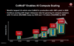
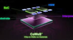
As semiconductor scaling slowed and system performance became increasingly constrained by data movement rather than raw compute, advanced packaging emerged as a decisive lever. Among these technologies, TSMC’s CoWoS (Chip-on-Wafer-on-Substrate) represents a turning point in how high-performance systems are … Read More