You are currently viewing SemiWiki as a guest which gives you limited access to the site. To view blog comments and experience other SemiWiki features you must be a registered member. Registration is fast, simple, and absolutely free so please,
join our community today!
In a significant example of how high-tech manufacturing can embrace environmental stewardship without compromising operational excellence, Taiwan Semiconductor Manufacturing Company has launched a sustainability initiative within its advanced packaging operations that both reduces waste and generates meaningful… Read More
In a landmark presentation at the 2025 IEEE Electronic Components and Technology Conference (ECTC), TSMC unveiled a groundbreaking advancement in thermal management: Direct-to-Silicon Liquid Cooling integrated directly onto its CoWoS® platform. This innovation, detailed in the paper “Direct-to-Silicon Liquid… Read More
In a significant milestone for the semiconductor industry, Teradyne was honored as the 2025 TSMC Open Innovation Platform® Partner of the Year for TSMC 3DFabric® Testing. This award, announced on September 25, 2025, underscores the deep collaboration between Teradyne, a leader in automated test equipment and robotics, and… Read More
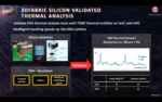
Today Alchip Technologies, a Taipei-based leader in high-performance and AI computing ASICs, announced a significant milestone with the successful tape-out of its 3D IC test chip. This achievement not only validates Alchip’s advanced 3D IC ecosystem but also positions the company as a frontrunner in the rapidly evolving field… Read More
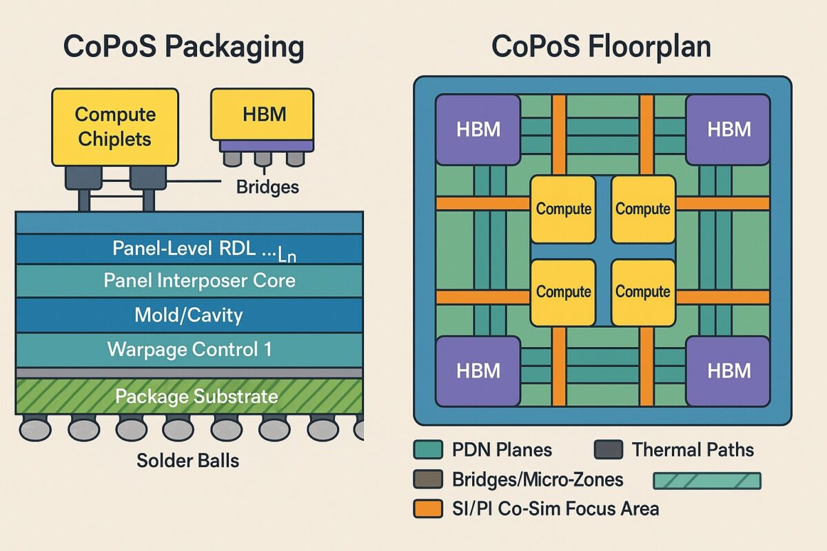
Chip on Panel on Substrate, often shortened to CoPoS, extends the familiar idea of chip on carrier packaging by moving the redistribution and interposer style structures from circular wafers to large rectangular panels. The finished panel assembly is then mounted on an organic or glass package substrate. This shift from round
…
Read More
Alchip Technologies Ltd., a global leader in high-performance computing (HPC) and artificial intelligence (AI) ASIC design and production services, continues its trajectory of rapid growth and technical leadership by pushing the boundaries of advanced-node silicon, expanding its global design capabilities, and building… Read More
The main program for the 70th IEDM opened on Monday morning in San Francisco with an excellent keynote from Dr. Yuh-Jier Mii, Executive Vice President and Co-Chief Operating Officer at TSMC. Dr. Mii joined TSMC in 1994. Since then, he has contributed to the development and manufacturing of advanced CMOS technologies in both fab
…
Read More
At the recent TSMC OIP Ecosystem Forum in Santa Clara, there was an important presentation that laid the groundwork for a great deal of future innovation. Alchip and its IP and EDA partner Synopsys presented Efficient 3D Chiplet Stacking Using TSMC SoIC. The concept of 3D, chiplet-based design certainly isn’t new. SemiWiki maintains… Read More
The ASIC business has always been a key enabler of the semiconductor industry but it is a difficult business. In my 40 years I have seen many ASIC companies come and go but I have never seen one like Alchip.
Alchip Technologies Ltd. was founded more than 20 years ago, about half way through my career. I know one of the founders, a fiercely… Read More
At the 2024 TSMC OIP Ecosystem Forum, one of the technical talks by TSMC focused on maximizing 3DIC design productivity and rightfully so. With rapid advancements in semiconductor technology, 3DICs have become the next frontier in improving chip performance, energy efficiency, and density. TSMC’s focus on streamlining the… Read More