


From DIP to Advanced, semiconductor packaging has become strategic
For ease of reading – I am going to be splitting this primer into two parts. First is the technical overview of everything. Next will be the company-specific writeups that follow over time – specifically Teradyne, Formfactor, Advantest, and Camtek. Maybe Keysight and others over time. The concepts in this primer will likely be referenced over and over. This is a primer I wish someone had written sooner, as this will become a must-know in semiconductors going forward.
Why is Packaging Important Now
Packaging used to be an afterthought in the process of semiconductor manufacturing. You made the little piece of silicon magic, and then you attached it and moved on your merry way. But as Moore’s law has stretched, engineers realized that they could utilize all parts of their chip including the packaging to make the best possible product. Improving packaging gives you significant benefits, as there are thicker metal pieces for better conductivity, and I/O (input/output) problems are still one of the greatest issues for semiconductors.
What is more amazing is that none of the packaging companies were considered as important as the traditional front-end manufacturing processes in the past. The packaging supply chain was often considered “back-end” and viewed as a cost center, similar to the front office and back office in banking. But now as the front end struggles to scale geometry, a whole new field of focus has emerged, and this is the emphasis on packaging. We will discuss the variety of processes so you will never feel lost again while looking into this segment of semicap and understand what 2.5D or 3D packaging means.
A Brief History of Packages
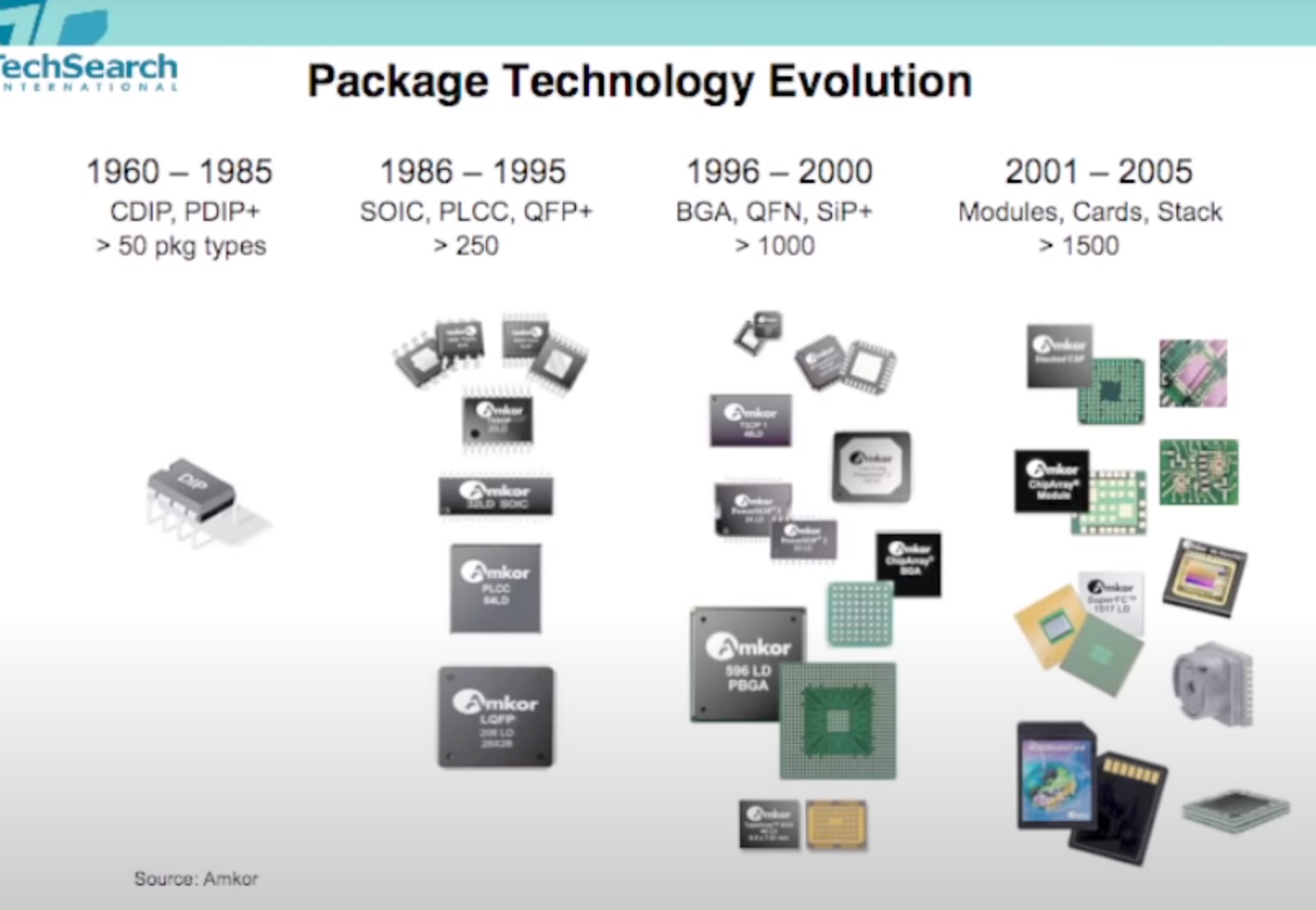
This is a brief hierarchy of package technologies I found from this wonderful Youtube lecture. If you have some time this series is worth a watch. Importantly it shows the hierarchy, of technology from past to present.

There is clearly a lot of different package technologies, but we are going to go over the simplistic ones that broadly representative of each type and then bring it slowly to the present. I also really like this high-level overview below (it’s dated but still correct).
In the very beginning of packaging, things were often in ceramic or metal cans and hermetically (airtight) sealed for maximum possible reliability. This mostly applied to aerospace and military functions, where the highest level of reliability was required. However, this was not really feasible for most of our day to day use cases, and so we started to use plastic packaging and dual in-line packaging (DIP).
DIP Packaging (1964-1980s)
DIP was introduced in the 1970s and became law of the land for a decade before surface mount technologies were introduced. DIPs used plastic enclosures around the actual semiconductor and had two parallel rows of protruding electrical pins called leadframes that was connected to a PCB (printed circuit board) below.

DIP like so many early semiconductor inventions was created in 1964 by Fairchild semi. DIP packages are kind of iconic in a retro way, and the design choices are understandable. The actual die would be completely sealed in resin, so it leads to high reliability and low cost, and many of the first iconic semiconductors were packaged in this way. Notice that the die is connected to the external lead frame via wire, and this makes this a “wire-bonding” method of packaging. More on that later.
Below is the Intel 8008 – effectively one of the first modern microprocessors. Notice it’s iconic DIP packaging. So if you ever see those funky photos of semiconductors that look like little spiders, this is just a DIP package class semiconductor.

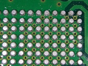
Each of those little metal pieces then gets soldered onto a PCB where it makes contact with other electrical components and the rest of the system. Below is how the package is soldered onto a PCB board.
The PCB itself is often made of copper or other electrical components laminated by a non-conductive material. PCBs can then route electricity from place to place and let the components interconnect and talk to each other. Notice the fine lines between each of the circuits that are soldered to the PCB, those are embedded wires that serve as conduits from piece to piece. That is the “package” part of the packaging, and PCBs are the highest level of packaging.
While there are other renditions of DIP – it’s actually time to move onto the next paradigm of packaging technology that began in the 1980s, or Surface Mount Packages.
Surface Mount Packaging (1980s-1990s)
Instead of mounting the products via DIP, the next step-change was the introduction of surface mounted technology (SMT). As implied, the package is mounted directly onto the surface of the PCB and allows for more components and lower cost on a piece of substrate. Below is a picture of a typical surface-mounted package.
 Design | PREDICTABLE DESIGNS")
There are many variations of this package, and this was a workhorse for a long time in the heyday of semiconductor innovation. Something I want you to notice is that instead of the two lead frames that mount to the PCB, now there are 4 surfaces on all sides that are mounted. This follows the general desire of packaging, to take up less space and increase connection bandwidth or I/O. Each additional advancement will have that in mind and is a pattern to watch for.
This process was once manual but now is highly automated. Additionally, this actually created quite a slew of issues for PCBs such as popcorning. Popcorning the package is when moisture inside the plastic package is heated during the soldering process and the moisture causes issues in the PCB due to rapid reheating and cooling. Another thing to note is that with each increase in the packaging process there is an additional increase in complexity and failure.
Ball Grid Packaging and Chip Scale Packaging (1990s – 2000s)
As the demands of semiconductor speed continue to pick up, so does the need for better packaging. While QFN (quad-flat no-leads) and other Surface Mounted technologies clearly continue to proliferate, I want to introduce you to the beginning of a package design that we will have to know about in the future. This is the beginning of the solder balls – or broadly Ball Grid Array (BGA) packaging.
This is what the ball grid array looks like and can directly mount a piece of silicon to a PCB or substrate from below rather than just taping down the corners on all 4 ends like the previous surface mounted technology.

So this is just another continuation of the trend I listed above, taking less space and having more connection. Now instead of a wire finely connecting the package on each side, we are now directly attaching one package to another. This leads to increased density, better I/O (a synonym for performance), and now the added complexity of how do you check to see if a BGA package is working. Up until this point, the packages were primarily visually inspected and tested. Now we can’t see the package so there was no way to test. Enter X-rays for inspection, and eventually more sophisticated techniques.
Solder bumps are also something I want you to remember as the primary way things are bonded to each other now, as this is the most common type of package interconnection pattern.
Modern Packaging (2000s-2010s)
We are now stepping into the modern era of packaging. Many of the packaging schemes described above are still in use today, however, there are increasingly more package types that you will start to see and those will become more relevant in the future. I will start to describe these now. To be fair many of these upcoming technologies were invented in previous decades, but because of cost, were not widely used until later.
Flip Chip
This is one of the most common packages you will likely read or hear about. I’m happy I can define it for you because I’ve never had a satisfying explanation in a primer I’ve read so far. Flip Chip was invented by IBM very early on and often will be abbreviated as C4. In the case of flip-chip, it really isn’t a stand-alone package form factor but rather a style of packaging. It’s pretty much just whenever there is a solder bump on a die. The chip is not wire bonded for interconnect but flipped to face the other chip with a connecting substrate in between, therefore “flip-chip”.
I don’t expect you to understand just from that awkward sentence, and I want to give you an example from Wikipedia, who has actually some of the best work on this I’ve seen. Let’s walk you through the steps.
- ICs are created on the wafer
- Pads are metalized on the surface of the chip

- A solder dot is deposited on each of the pads


- Chips are cut
- Chips are flipped and positioned so that the solder balls are facing circuitry


- Solder balls are then remelted

- Mounted chip is underfilled with an electrically insulating adhesive


Wire Bond
Notice how flip-chip is different from wirebond. Remember that DIP package up top? That was wire bonding, where a die uses wires to be bonded to another metal that is then soldered to the PCB. Once again wire bonding is not a specific technology, but rather an older set of technologies that encompasses a lot of different types of packaging. I think it’s best described in relief to flip-chip. Wirebond is a precursor to flip-chip to be clear.
Honest if you’ve made it this far – you’re a champ. I think that really is all you need to know for this segment. There is a large number of variations of each form factor and just think of these as the overarching themes that dictate them. KLIC by the way is the market leader in this segment, and when you think of old packaging technology you should think of them.
Advanced Packaging (2010s to Today)
We are ever so slowly creeping into the “advanced packaging” semiconductor era, and I wanted to maybe touch on some higher-level concepts now. There are actually various levels of “package” that kind of fit within this thought process. Most of the packaging we have talked about before has been focused on chip package to PCB, but the beginning of advanced packaging really starts with the phone.
The mobile phone in a lot of ways is the huge precursor to so many aspects of advanced packaging. It makes sense! A phone in particular is a lot of silicon content in the smallest space possible, much denser than your laptop or computer. Everything must be passively cooled, and of course as thin as possible. Every year Apple and Samsung would announce a faster but more importantly thinner phone, and this pushed packaging to new limits. Many of the concepts that I will discuss began in the smartphone package and has now pushed itself to the rest of the semiconductor industry.
Chip Scale Packaging (CSP)
Chip scale packaging is actually a bit broader than it sounds and originally means chip-size packaging. The technical definition is a package that has no greater than 1.2x the size of the die itself, and it must be single-die and attachable. I actually have already introduced you to the concept of CSP, and that is through flip-chips. But CSP was really taken to the next level via smartphones.
The 2010s made CSP law of the land, everything in this photo is 1.2x the size of the chip die, and is focused on saving as much space as possible. There are a lot of different flavors of the CSP era with flip-chip, right substrate, and other technologies all part of this classification. But I don’t think knowing the specifics are of many benefits to you.
Wafer-level packaging (WLP)
But there is one level smaller – and this is the “ultimate” chip scale packaging size, or at wafer-level packaging. This is pretty much just putting the packaging on the actual silicon die itself. The package IS the silicon die. It’s thinner with the highest level of I/O, and obviously very hot and hard to manufacture. The advanced packaging revolution is currently at the CSP scale, but the future is all focused on the wafer.
It’s an interesting evolution, the package was something that got subsumed by the actual silicon itself. The chip is the package and vice versa. This is really expensive compared to just soldering some balls onto the chip, so why we are doing this? Why is there such an obsession with advanced packaging now?
Advanced Packaging: The Future
This is a culmination of the trends I have been writing about for a long time. Heterogeneous computing is not only the story of specialization, but how we put all those specialized pieces together. Advanced packaging is that crucial enabler that makes it all work.
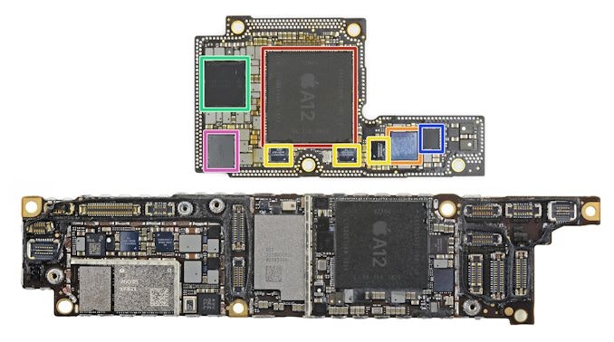
Let’s look at the M1 – a classic heterogeneous compute configuration, specifically with their unified memory structure. The M1 to me is not a “wow cool” moment but a singular moment of pre and post for Heterogeneous compute. The M1 is ringing in what the future looks like, and many will be following Apple’s suit pretty shortly. Notice the actual SOC (system on chip) is not heterogeneous – but the custom package that brings the memory close to the SOC is.

Another great example of a very good advanced package is the new A100 by Nvidia. Once again notice no wires on the PCB.
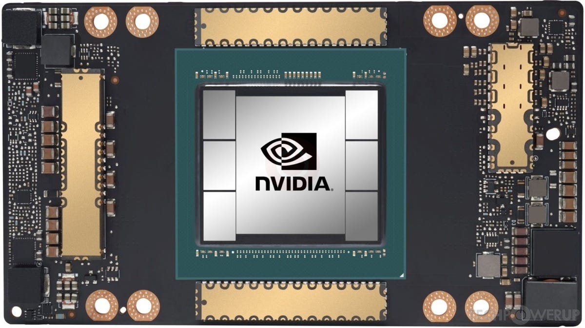
Check this quote from their whitepaper.
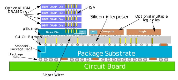
Rather than requiring numerous discrete memory chips surrounding the GPU as in traditional GDDR5 GPU board designs, HBM2 includes one or more vertical stacks of multiple memory dies. The memory dies are linked using microscopic wires that are created with through-silicon vias and microbumps. One 8 Gb HBM2 die contains over 5,000 through-silicon via holes. A passive silicon interposer is then used to connect the memory stacks and the GPU die. The combination of HBM2 stack, GPU die, and Silicon interposer are packaged in a single 55mm x 55mm BGA package. See Figure 9 for an illustration of the GP100 and two HBM2 stacks, and Figure 10 for a photomicrograph of an actual P100 with GPU and memory.
The takeaway here is that the best silicon in the world is being made one type of way, and this revolution is not stopping. Let’s learn a little bit more about the words above and translate this into English. First some more about the two overarching categories of Advanced packaging, 2.5D, and 3D packages.
2.5D Packaging
2.5D is kind of like a turbo version of the flip-chip we mentioned above, but instead of stacking a single die onto a PCB, die are stacked on top of a single interposer. I think this graphic puts it well.

2.5D is like having a basement door into your neighbor’s house and physically is either a bump or a TSV (through silicon vias) into the silicon interposer beneath you, and that connects you to your neighbor. It isn’t faster than your actual on-chip communication, but since your net output is decided on the total package performance, the lowered distance and increased interconnection between the two silicon pieces outweigh the downsides of not having everything on a single SOC. The benefit of this is you can use “known good die” – or smaller pieces of silicon to piece together larger more complex packages very quickly. It would be better to all be done on one piece of silicon, but this process makes fabrication a lot easier especially at smaller sizes.
Those little pieces of silicon – are often called “chiplets” that you’ve heard all about. Now you can get chiplets of small functional blocks of silicon designed to be combined together, connect them on a single flat silicon substrate, and boom! 2.5D Package at your service.
Chiplets and 2.5D packaging are probably going to be used for a long while, it has a very workhorse like quality to it and likely will be easier to make than outright 3D and much cheaper as well. Additionally, it can scale well and can be reused with new chiplets thus making new chips in the same package format by just replacing the chiplet. The new Zen3 improvements are an of this, where the package is similar but some of the chiplets got upscaled. However this still kind of stops short at the final version of packaging, which is 3D
3D Packaging
3D packaging is the holy grail, the ultimate ending of packaging. Think of it this way, now instead of having all those separate little houses on the ground that are 1 story tall and connected by basements, we can just have one giant skyscraper that is custom made with whatever process is needed to fit the function. This is 3D Packaging – and now all the packaging is done on the piece of silicon itself. It is the single fastest and power-efficient way to drive larger more complex structures that are feature built to the task, and will “extend” Moore’s law significantly. We may not be able to get more feature shrink in the future, but now with 3D packaging we still could improve our chips into the future similar to Moore’s law of old.
And what’s interesting is we have a clear example of an entire semiconductor market that went 3D – Memory. Memory’s push into 3D structures is a very good indication of what’s to come. Part of the reason why NAND had to go 3D was that they struggled to scale at smaller geometry. Imagine memory as a large 3D skyscraper, and each of the floors is kept together by an elevator. These are called “TSV”s or Through silicon vias.

This is what the future looks like, and it’s even possible we will be stacking GPU/CPU chips on each other or stacking memory on CPU. This is the final frontier and one we are quickly approaching. You will likely start to see 3D packaging pop up over and over in the next 5 years.
A Quick Overview of 2.5D/3D Packaging Solutions
Instead of going much further into 3D and 2.5D packaging, I think it’s best to just lay out some processes that are being used and you might have heard before. I want to focus here on processes done by fabs, which are the ones that drive 3D/2.5D integration forward.
This is seemingly the workhorse of the 2.5D integration process and was pioneered by Xilinx.
This process is mostly focused on putting all the logic dies onto a silicon interposer, and then onto a package substrate. Everything is connected via microbumps or balls. This is a classical 2.5D structure.
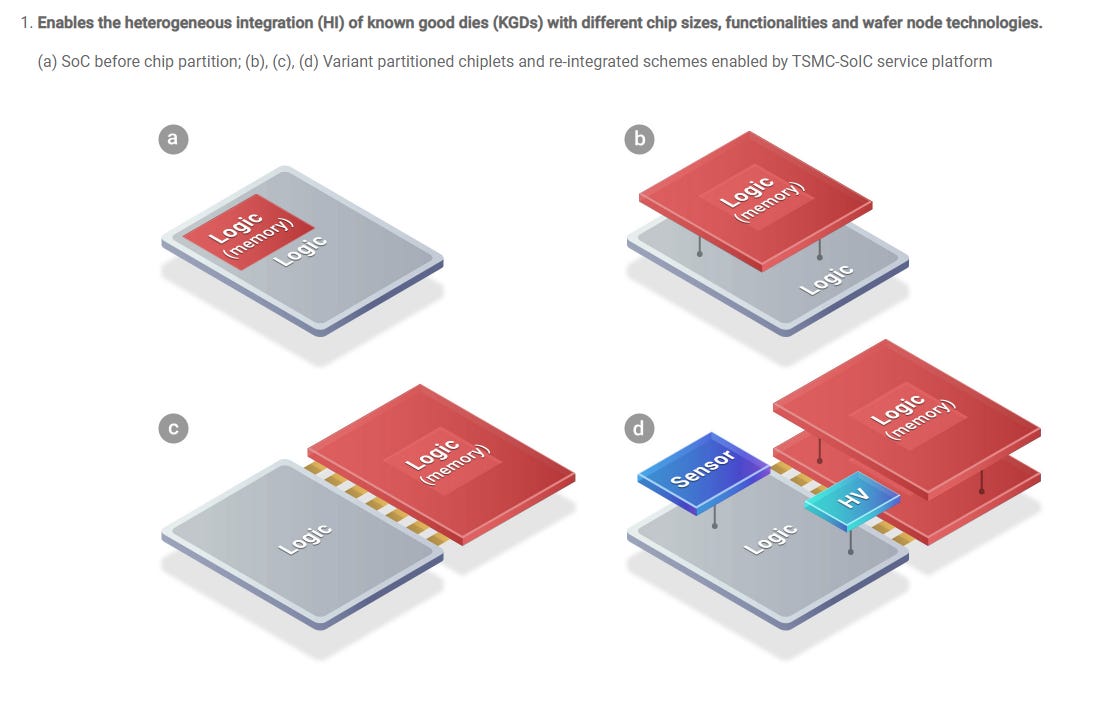
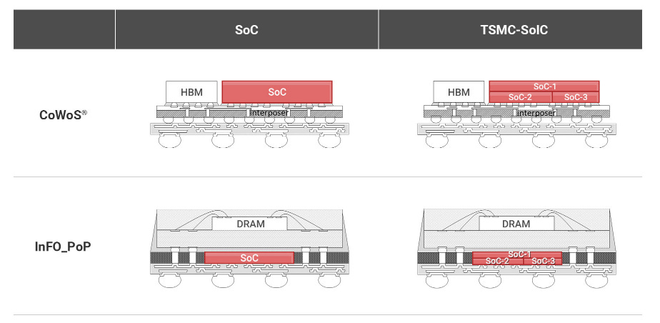
This TSMC’s 3D Packaging platform, and is the relatively new kid on the block.
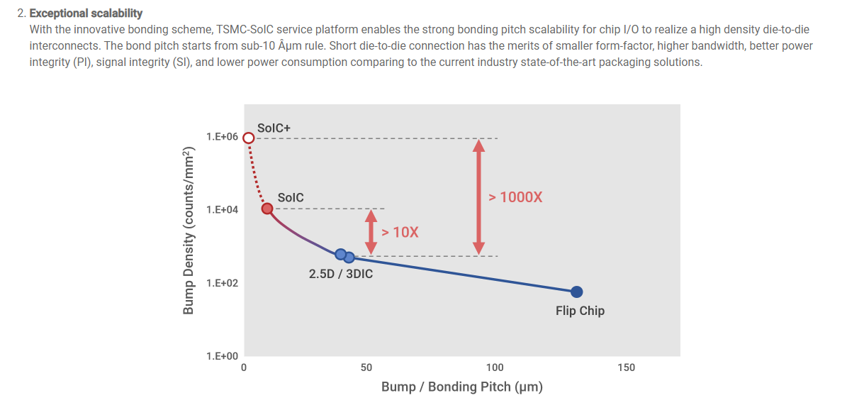
Notice this amazing graph on bump density and bonding pitch, SoIC is not even close to Flipchip or 2.5D in size and rather is pretty much a front end process in terms of density and feature size.
This is a good comparison of their technologies, but note that the SoIC actually has a chip on chip stacking akin to 3D stacking, instead of the interposer 2.5D integration.
Samsung XCube
Samsung has become a much more important foundry partner in recent years, and of course not to be outmatched Samsung has a new 3D packaging scheme. Check out the video for their XCube below.
There isn’t exactly a lot of information here, but I want to highlight that the A100 was fabbed on the Samsung process, so this is likely the technology powering Nvidia’s recent chip. Additionally of all the companies here, Samsung likely has the most experience with TSVs due to their 3D memory platform, so clearly, they know what they are doing.
Intel Foveros
Last but not least is Intel’s Foveros 3D packaging. We will likely see more implementations from Intel in their “hybrid CPU” process from their future 7nm and beyond generations. They have been pretty explicit at Architecture days that this is their focus going forward.
Something that is interesting is that there really isn’t much differentiation between Samsung, TSMC, or Intel in the 3D process.
Winners from the Advanced Packaging Revolution
So if you remember this post that was the introduction to the semicap series, Advanced packaging firmly is the “mid-end” that I reference. Why this is so interesting is because this is all incremental growth.
In the past, packaging estimates were excluded from WFE (Wafer Fab Equipment) estimates annually, but as of 2020, they are starting to include wafer-level packaging. This is kind of the signal for the wind shift and why the mid-end is very interesting from here. Another definition for Mid-end is Back End of Line (BOEL). For a more in-depth discussion of packaging-related companies, refer to my packaging stocks follow-up.
Subscribe to Fabricated Knowledge
Let’s learn more about the world’s most important manufactured product. Meaningful insight, timely analysis, and an occasional investment idea.


TSMC CoWoS versus Intel EMIB Semiconductor Packaging