You are currently viewing SemiWiki as a guest which gives you limited access to the site. To view blog comments and experience other SemiWiki features you must be a registered member. Registration is fast, simple, and absolutely free so please,
join our community today!
In this episode of the Semiconductor Insiders video series, Dan is once again joined by Anna Fontanelli, founder and CEO of MZ Technologies. In this discussion, more details of the challenges presented by advanced packaging and multi-die design are explored. Anna provides details of what’s involved in architectural … Read More
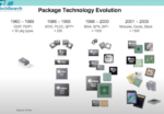
From DIP to Advanced, semiconductor packaging has become strategic
For ease of reading – I am going to be splitting this primer into two parts. First is the technical overview of everything. Next will be the company-specific writeups that follow over time – specifically Teradyne, Formfactor, Advantest, and Camtek
…
Read More
We introduced you to Semitracks last week with an interview of their CEO, Chris Henderson. This week, we thought it might be worthwhile to continue that introduction with an overview of one of their more popular online and in-houses courses:
Introduction to Semiconductor Processing.
One of the big challenges in our industry for… Read More
Continuing to find new ways to extend Moore’s Law, the foundry and technology leader is ready to show off its wafer level system integration prowess with two scalable platforms targeting key growth markets.
CoWoS® (Chip-On-Wafer-On-Substrate) goes after high-performance applications, providing the highest bandwidth and… Read More