

Semicap is in some ways the unsung hero of American global dominance in semiconductors. The US punches above its weight in terms of market share compared to demand, but specifically in three categories. EDA, IP, and Equipment.

I hope to write about everything there can be said about semiconductors, and EDA is a place I understand a bit but not as much as I’d like. I still really like the Scuttleblurb EDA primer – and refer back to it from time to time. But Semicap – that is a place I feel pretty confident about, and I think the industry structure, capital returns, and defensiveness of the businesses is truly attractive. It’s a great subsector and always seems to reasonably priced.
Industry Overview and Map
First – I am going to start with this industry map and kind of break it down further. I really like this simplistic semiconductor industry map @Fritz844 made on Twitter (he seems to have deleted it).

You can see here where the Semicap companies exist – and who their key customers are. There is another level deeper I wanted to make a graphic for. Also “mid-end” semicap is something that is kind of emerging and new, so if you haven’t really heard of it before that is okay. I would put advanced packaging firmly in this segment, and this is where the back end is starting to look a lot more like the front end. More on that later.

I think this is a decent industry map, with the customers on one end (purchasers) and the suppliers on the other (Semicap and materials). I think right now there is a bit more blurring of Semicap lines than there was in the past, with materials and mid-end kind of being the emerging points of relevance on the map. Obviously, the front end is going to continue to be the most important part, but with the end of Moore’s law, we increasingly need new materials, new technologies (advanced packaging!), and new methods to keep the pace of improvement constant. If you have no idea what Front End, Back End, or Mid End mean, that’s where the next part comes into play.
The 10,000+ foot view of Semicap
My favorite quick infographic on how a semiconductor is made is from the ASML Annual report. I will briefly walk through a few of the steps.
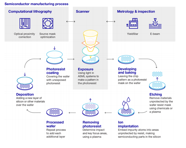
Let’s start with Photoresist. The photoresist is a light-sensitive polymer put on top of a silicon wafer, and when exposed to light it turns into a soluble material. The exposure to light step is called lithography, and using light, they can print materials onto the wafer. This process is similar to old fashioned photography and film, and the light is shone through a lens called a photomask and imprints it’s image onto the film or silicon wafer.
After exposure, you smooth out the resist using a bake, which helps development. Development is similar to developing a photo and uses aqueous bases to create the shape of the photoresist profile. Next comes either etching, deposition, or ion implantation. Each has a different role in building a semiconductor transistor pattern, such as subtracting, adding, or doping the substrate.
Etching is the most common, and etching is usually performed using wet chemicals or plasma and is commonly used to dig deeper trenches. The photoresist material resists the etching and protects the covered material, and then they can print the process onto the substrate.
Last is stripping the photoresist, to then move onto another cycle or step in the fabrication process. Each of these steps is often to just print a single layer. And many modern semiconductors can have hundreds of layers built on top of each other, and of course, any single mistake will create a defect in the semiconductor. This explains why they are obsessed with cleanliness in the fabs. A single micron of dust will destroy a die and ruin yields.
For me – I think of building a semiconductor like laying a city filled with skyscrapers one floor at a time. Each step in the process either adds or subtracts a floor. After hundreds of steps, you then take a step back and you have your fully built “city”, complete with the hundreds of miniature skyscraper-like transistors.
Everything I just described here is what is called the front end of semicap. The front end usually refers to the equipment that goes into the physical transistor creation from silicon and tends to be the largest source of spending for fabs. The emerging “mid-end” is post transistor, but pre-die-cutting or advanced packaging.
With wafer-level advanced packaging such as CoWoS processes and more, parts of packaging that were firmly in the back end historically are moving towards the front end. This is really important and likely one of the best opportunities in growth and misunderstood businesses for now.
Lastly the backend. After the semiconductor leaves the fab, the product is not done yet. There are more steps of assembly and testing that have to go into making a working end product from pieces of silicon. Even the typical CPU core you see has some level of packaging applied to it after fabrication. This has historically tended to be more cyclical and considered a worse business at the end of the tailwhip of the semiconductor supply chain. But with the importance of packaging rising in Heterogeneous compute, many back-end companies have been thrown a strategic lifeline.
Each of these steps is “owned” by a particular company. We will be diving into market share, positioning, and company descriptions in focused paid write-ups – but for now, know that the top 5 semicap companies have approximately ~65% market share. This is an oligopoly and a profitable one at that. There are some niches in each business that are truly wonderful. I think you’ll also learn a lot about the core science, the barriers to entry, and some of the most wonderful technology we’ve come up with to date. These will all be paid posts to come.
Subscribe to Fabricated Knowledge
Let’s learn more about the world’s most important manufactured product. Meaningful insight, timely analysis, and an occasional investment idea.
Share this post via:


Enhancing Multi-Domain System Simulation with FMI Co-Simulation