TSMC’s 3DFabric initiative was a big focus at the symposium, as it should be. I remember when TSMC first went public with CoWos the semiconductor ecosystem, including yours truly, let out a collective sigh wondering why TSMC is venturing into the comparatively low margin world of packaging. Now we know why and it is absolutely brilliant!
In 2012 TSMC introduced, together with Xilinx, the by far largest FPGA available at that time, comprised of four identical 28 nm FPGA slices, mounted side-by-side, on a silicon interposer. They also developed through-silicon-vias (TSVs), micro-bumps and re-distribution-layers (RDLs) to interconnect these building blocks. Based on its construction, TSMC named this IC packaging solution Chip-on-Wafer-on-Substrate (CoWoS).
This building blocks-based and EDA-supported packaging technology has become the de-facto industry standard for high-performance and high-power designs. Interposers, up to three stepper fields large, allow combining multiple die, die-stacks and passives, side by side, interconnected with sub-micron RDLs. Most common applications were combinations of a CPU/GPU/TPU with one or more high bandwidth memories (HBMs).
In 2017 TSMC announced the Integrated FanOut technology (InFO). It uses, instead of the silicon interposer in CoWoS, a polyamide film, reducing unit cost and package height, both important success criteria for mobile applications. TSMC has already shipped tens of millions of InFO designs for use in smartphones.
In 2019 TSMC introduced the System on Integrated Chip (SoIC) technology. Using front-end (wafer-fab) equipment, TSMC can align very accurately, then compression-bond designs with many narrowly pitched copper pads, to further minimize form-factor, interconnect capacitance and power.
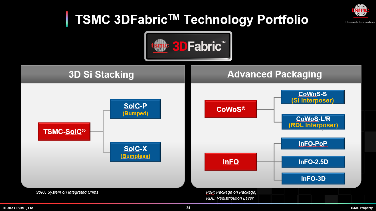
Today TSMC has 3DFabric, a comprehensive family of 3D Silicon Stacking and Advanced Packaging Technologies. Here are the TSMC related accomplishments from the briefing:
- TSMC 3DFabric consists of a variety of advanced 3D Silicon Stacking and advanced packaging technologies to support a wide range of next-generation products:
- On the 3D Si stacking portion, TSMC is adding a micro bump-based SoIC-P in the TSMC-SoIC® family to support more cost-sensitive applications.
- The 2.5D CoWoS® platform enables the integration of advanced logic and high bandwidth memory for HPC applications, such as AI, machine learning, and data centers. InFO PoP and InFO-3D support mobile applications and InFO-2.5D supports HPC chiplet integration.
- SoIC stacked chips can be integrated in InFO or CoWoS packages for ultimate system integration.
- CoWoS Family
- Aimed primarily for HPC applications that need to integrate advanced logic and HBM.
- TSMC has supported more than 140 CoWoS products from more than 25
- All CoWoS solutions are growing in interposer size so they can integrate more advanced silicon chips and HBM stacks to meet higher performance requirements.
- TSMC is developing a CoWoS solution with up to 6X reticle-size (~5,000mm2) RDL interposer, capable of accommodating 12 stacks of HBM memory.
- InFO Technology
- For mobile applications, InFO PoP has been in volume production for high-end mobile since 2016 and can house larger and thicker SoC chips in smaller package form factor.
- For HPC applications, the substrateless InFO_M supports up to 500 square mm chiplet integration for form factor-sensitive applications.
- 3D Silicon stacking technologies
- SoIC-P is based on 18-25μm pitch μbump stacking and is targeted for more cost-sensitive applications, like mobile, IoT, client, etc.
- SoIC-X is based on bumpless stacking and is aimed primarily at HPC applications. Its chip-on-wafer stacking schemes feature 4.5 to 9μm bond pitch and has been in volume production on TSMC’s N7 technology for HPC applications.
- SoIC stacked chips can be further integrated into CoWoS, InFo, or conventional flip chip packaging for customers’ final products.

- 3DFabric™ Alliance and 3Dblox Standard
- At last year’s Open Innovation Platform®(OIP) Forum, TSMC announced the new3DFabric™ Alliance, the sixth OIP alliance after the IP, EDA, DCA, Cloud, and VCA alliances, to facilitate ecosystem collaboration for next-generation HPC and mobile designs by:
- Offering 3Dblox Open Standard,
- Enabling tight collaboration between memory and TSMC logic, and
- Bringing Substrate and Testing Partners into Ecosystem.
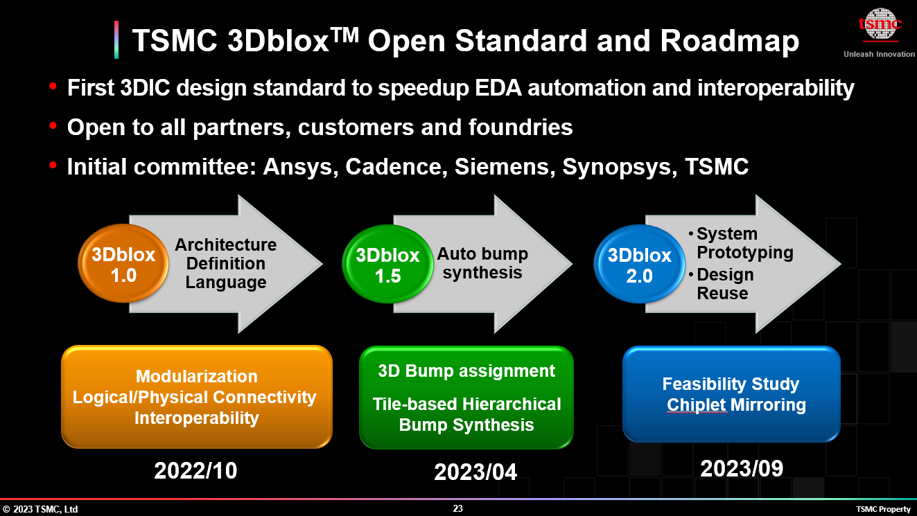
- TSMC introduced 3Dblox™ 1.5, the newest version of its open standard design language to lower the barriers to 3D IC design.
- The TSMC 3Dblox is the industry’s first 3D IC design standard to speed up EDA automation and interoperability.
- 3Dblox™ 1.5 adds automated bump synthesis, helping designers deal with the complexities of large dies with thousands of bumps and potentially reducing design times by months.
- TSMC is working on 3Dblox 2.0 to enable system prototyping and design reuse, targeting the second half of this year.
- At last year’s Open Innovation Platform®(OIP) Forum, TSMC announced the new3DFabric™ Alliance, the sixth OIP alliance after the IP, EDA, DCA, Cloud, and VCA alliances, to facilitate ecosystem collaboration for next-generation HPC and mobile designs by:

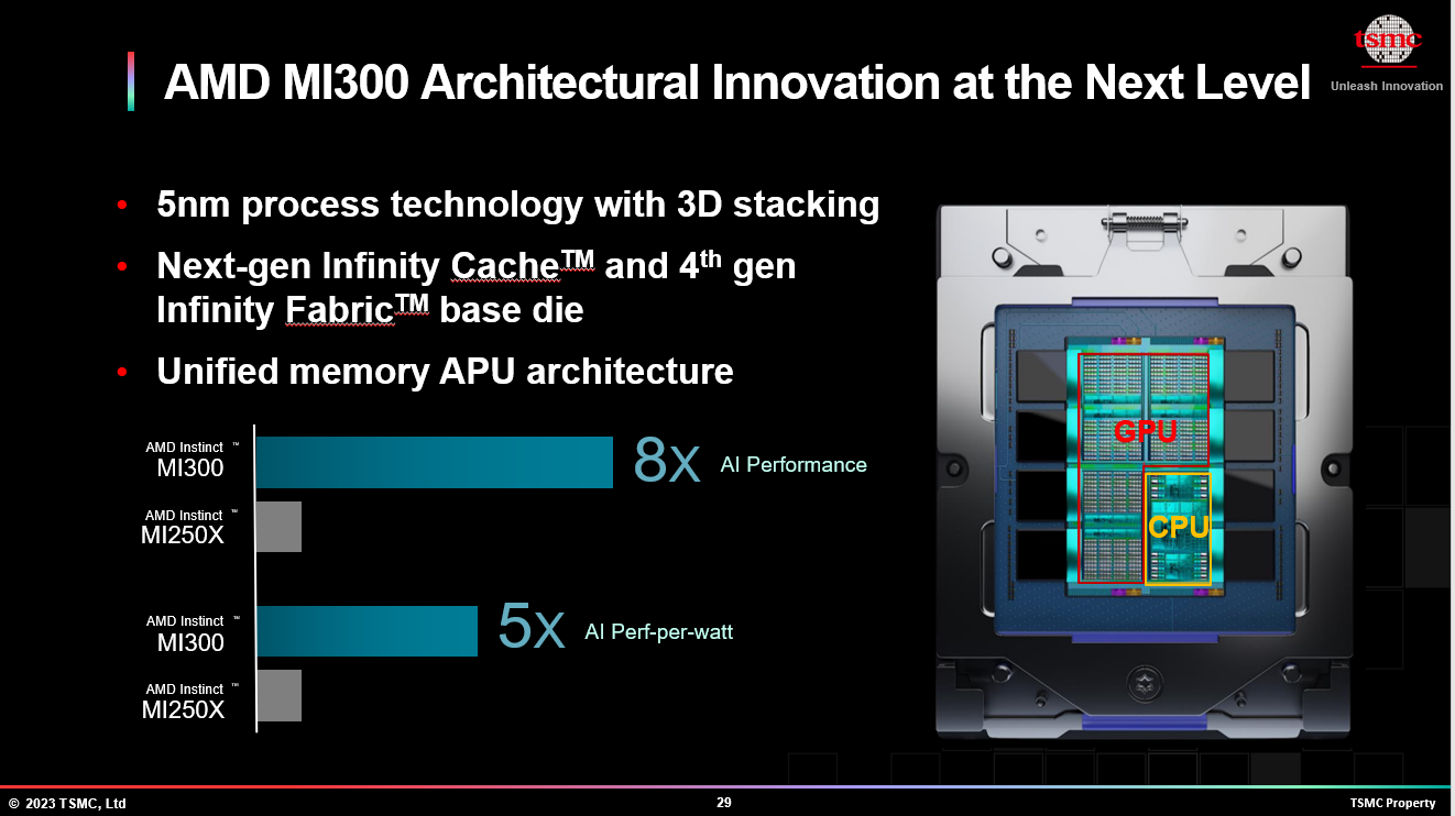
Above is an example of how TSMC 3DFabric technologies can enable an HPC chip. It also supports my my opinion that one of the big values of the Xilinx acquisition by AMD was the Xilinx silicon team. No one knows more about implementing advanced TSMC packaging solutions than Xilinx, absolutely.
Also Read:
TSMC 2023 North America Technology Symposium Overview Part 1
TSMC 2023 North America Technology Symposium Overview Part 2
TSMC 2023 North America Technology Symposium Overview Part 4
TSMC 2023 North America Technology Symposium Overview Part 5
Share this post via:


Comments
There are no comments yet.
You must register or log in to view/post comments.