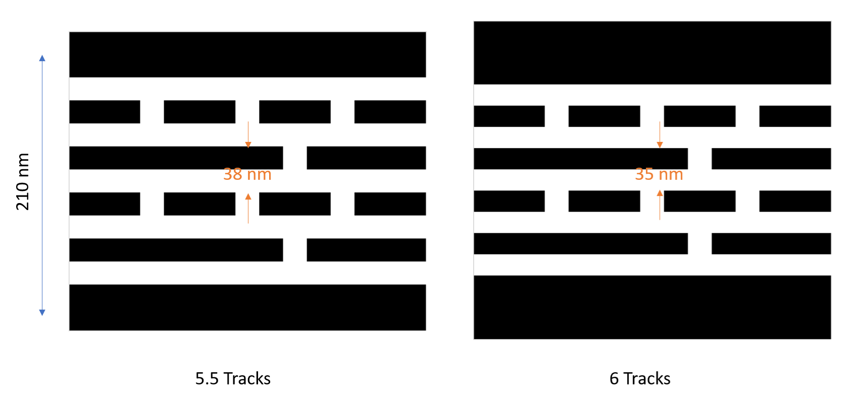
At IEDM 2019, TSMC revealed two versions of 5nm standard cell layouts: a 5.5-track DUV-patterned version and a 6-track EUV-patterned version [1]. Although the metal pitches were not explicitly stated, later analyses of a 5nm product, namely, Apple’s A15 Bionic chip, revealed a cell height of 210 nm [2]. For the 6-track cell, this indicates a metal track pitch of 35 nm, while for the 5.5-track cell, the pitch is 38 nm (Figure 1). Just a 3 nm difference in pitch matters a lot for the patterning approach. As will be shown below, choosing the 5.5-track cell for DUV patterning makes a lot of sense.

Figure 1. 210 nm cell height means 38 nm track pitch for 5.5 tracks (left) or 35 nm track pitch for 6 tracks (left).
Extending the 7nm DUV Approach to 5nm
The 5.5-track metal pitch of 38 nm is at the limit of DUV double patterning. It can therefore reuse the same approach used in 7nm, where the 6-track cell metal pitch was 40 nm [3]. This can be as simple as self-aligned double patterning followed by two self-aligned cut blocks, one for each material to be etched (core or gap) (Figure 2). The minimum pitch of the cut blocks (for each material) is 76 nm, allowing a single exposure.

Figure 2. SADP followed by two self-aligned cut blocks (one for the core material, one for the gap material). Process sequence from left to right: (i) SADP (core lithography followed by spacer deposition and etchback, and gapfill; (ii) cut block lithography for exposing gap material to be etched; (iii) refill of cut block for gap material; (iv) cut block lithography for exposing core material to be etched; (v) refill of cut block for core material. Self-aligned vias (not shown) may be partially etched after the block formation [4].
In lieu of SADP, SALELE [5] may be used instead. This would add an extra mask for the gap material, resulting in a total of four mask exposures needed.
Going Below 38 nm Pitch: Hitting the Multipatterning Barrier
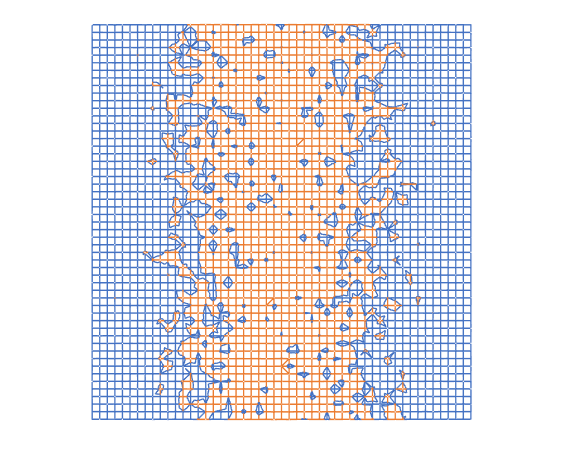
For the 3nm node, it is expected that the metal track pitch will go below 30 nm [6]. Any pitch below 38 nm would entail the use of substantially more DUV multipatterning [7]. Yet a comparable amount of multipatterning could also be expected even for EUV, as the minimum pitch from photoelectron spread can be effectively 40-50 nm for a typical EUV resist [8,9]. The edge definition for a 25 nm half-pitch 60 mJ/cm2 exposure is heavily affected by both the photon shot noise and the photoelectron spread (Figure 3).

Figure 3. 25 nm half-pitch electron distribution image exposed with an incident EUV dose of 60 mJ/cm2 (13 mJ/cm2 absorbed), with a 7.5 nm Gaussian blur to represent the electron spread function given in ref. [9]. A 1 nm pixel is used, with 4 secondary electrons per photoelectron.
5nm For All?
The 5.5-track cell provides an easy migration path from 7nm to 5nm using DUV double patterning. Potentially, this is one of the easier ways for Chinese companies to catch up at 5nm, although clearly that would be as far as they can take it.
References
[1] G. Yeap et al., IEDM 2019, Figure 5.
[2] https://www.angstronomics.com/p/the-truth-of-tsmc-5nm
[4] F. Chen, Self-Aligned Block Redistribution and Expansion for Improving Multipatterning Productivity, https://www.linkedin.com/pulse/self-aligned-block-redistribution-expansion-improving-frederick-chen-rgnwc/
[5] Y. Drissi et al., Proc. SPIE 10962, 109620V (2019).
[6] https://fuse.wikichip.org/news/7375/tsmc-n3-and-challenges-ahead/
[7] F. Chen, Extension of DUV Multipatterning Toward 3nm, https://semiwiki.com/lithography/336182-extension-of-duv-multipatterning-toward-3nm/, https://www.linkedin.com/pulse/extension-duv-multipatterning-toward-3nm-frederick-chen/
[8] F. Chen, Why NA is Not Relevant to Resolution in EUV Lithography, https://www.linkedin.com/pulse/why-na-relevant-resolution-euv-lithography-frederick-chen-ytnoc, https://semiwiki.com/lithography/344672-why-na-is-not-relevant-to-resolution-in-euv-lithography/
[9] T. Kozawa et al., JVST B 25, 2481 (2007).
This article first appeared in LinkedIn Pulse: Application-Specific Lithography: Patterning 5nm 5.5-Track Metal by DUV
Also Read:
Why NA is Not Relevant to Resolution in EUV Lithography
Huawei’s and SMIC’s Requirement for 5nm Production: Improving Multipatterning Productivity
Share this post via:


Is Intel About to Take Flight?