

The latest significant development in EUV lithography technology is the arrival of High-NA systems. Theoretically, by increasing the numerical aperture, or NA, from 0.33 to 0.55, the absolute minimum half-pitch is reduced by 40%, from 10 nm to 6 nm. However, for EUV systems, we need to recognize that the EUV light (consisting of photons) is ionizing, i.e., releases photoelectrons in absorbing materials. A 92 eV EUV photon, once absorbed, kicks off a ~70-80 eV photoelectron which gradually deposits most of the energy of the original photon [1]. The image information originally in the EUV photon density is replaced by the final migrated photoelectron density. The difference between minimum and maximum resist exposure is defined by where all the photoelectrons finally reach a particular energy cutoff. We also need to add the photoelectron number randomness which stems from the photon absorption randomness. The stochastic effects from the roughness lead to edge roughness, unpredictable edge position shifts, and even defects. All these considerations taken together require us to revisit the actual practical resolution for EUV lithography.
Photoelectron Model details
EUV light arriving at the wafer is a mixture of two components, one polarized parallel to the plane of incidence (TM), and one polarized perpendicular to the plane of incidence (TE). The photoelectron is emitted predominantly along the direction of polarization [2]. Purely unpolarized light should be a 50-50% mixture, but we may expect some departure because the mirrors in the EUV system may reflect near the Brewster angle [3]. With regard to lines being imaged, the photoelectrons along the TE polarization move along the lines, while the photoelectrons along the TM polarization move perpendicular to the lines. It is only the latter which degrades the image. Photoelectrons moving laterally effectively shift the image. Figure 1 shows the relative probability for a photoelectron to migrate a given distance to a 3 eV cutoff. This cutoff corresponds to the resist thickness loss following exposure and development [1].

Figure 1. Probability density for EUV photoelectron travel distance for an open-source resist, to a 3 eV energy cutoff [1].
The resist exposure at a given point will be affected by photoelectrons from a given distance away, weighted by the probability density for that distance, only for the TM case. The TE portion is taken to be unaffected by photoelectron migration as the photoelectron travels along the lines [3].
Picturing Photoelectron Spread
In a previous study [3], it was found that as pitch decreased below 40 nm, the image contrast, indicated by the normalized image log-slope (NILS), would degrade due to the photoelectron spread. As a reference, the photoelectron spread at 40 nm pitch can be pictured in Figure 2. The absorbed photon dose is affected by shot noise which directly affects the number of photoelectrons generated. At 5 mJ/cm2, roughly what is absorbed by 40 nm thick organic chemically amplified resist (CAR) at 30 mJ/cm2, the nominally unexposed region is penetrated by photoelectrons which can potentially print defects, and the nominally exposed region is thoroughly penetrated by photoelectron printing gaps. Raising the dose reduces this stochastic severity.

Figure 2. Photoelectron spread for 20 nm half-pitch vs absorbed dose. The orange portion indicates where the photoelectron density exceeds the half-pitch printing threshold. The pixel size is 1/40 of the pitch.
When the pitch is increased to 50 nm (Figure 3), the photoelectrons do not appear to spread as far stochastically, especially at the higher dose. This is due to the increased contrast, i.e., separation between maximum and minimum photoelectron densities in the image.
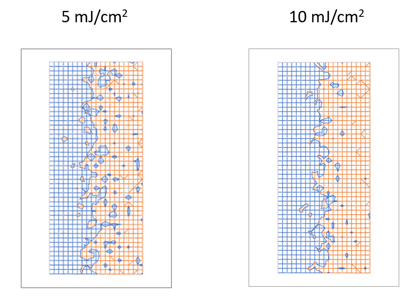
Figure 3. Photoelectron spread for 25 nm half-pitch vs absorbed dose. The orange portion indicates where the photoelectron density exceeds the half-pitch printing threshold. The pixel size is 1/40 of the pitch.
Redirecting the Determination of EUV Lithography Resolution
The EUV photoelectron spread probability density function shown in Figure 1 leads to a practical resolution limit of ~50 nm pitch for ~30 mJ/cm2, ~40 nm pitch for ~90 mJ/cm2 for a typical CAR. This is far above the expected resolution limit from 0.33 or 0.55 NA. The resolution limit should therefore not be primarily associated with the optics of the EUV system but in fact be tied to the photoelectron as well as secondary electron migration in the EUV resist. Moreover, the resolution is closely tied to the dose absorbed by the resist; a higher dose enables better resolution. This leads to a throughput tradeoff [4], requiring higher source power to compensate. The resolution of a given EUV resist must be characterized by calibrating low-energy electron scattering simulations [1,5] with resist thickness loss vs. electron dose measurements [1]. It must be kept in mind that while metal-containing resists are known for their enhanced EUV absorption [6], the SnOx-based resist does not necessarily have an advantage in photoelectron spread distance over the organic CAR [4]. Restrictions in elemental composition will prevent much deviation in the photoelectron spread function. As the resist will be the main determinant of EUV lithography resolution, less attention should be paid to the marketing of High-NA.
References
[1] A. Narasimhan et al., “What We Don’t Know About EUV Exposure Mechanisms,” J. Photopolym. Sci. and Tech. 30, 113 (2017).
[2] M. Kotera et al., Extreme Ultraviolet Lithography Simulation by Tracing Photoelectron Trajectories in Resist,” Jap. J. Appl. Phys. 47, 4944 (2008).
[3] F. Chen, Resolution Limit From EUV Photoelectron Spread, 2024 https://www.youtube.com/watch?v=3BIGo9UsIEA
[4] H. J. Levinson, Jpn. J. Appl. Phys. 61 SD0803 (2022).
[5] P. L. Theofanis et al., “Modeling photon, electron, and chemical interactions in a model hafnium oxide nanocluster EUV photoresist,” Proc. SPIE 11323, 113230I (2020).
[6] http://euvlsymposium.lbl.gov/pdf/2015/Posters/P-RE-06_Fallica.pdf).
This article first appeared in LinkedIn Pulse: Why NA is Not Relevant to Resolution in EUV Lithography
Also Read:
Huawei’s and SMIC’s Requirement for 5nm Production: Improving Multipatterning Productivity
ASML- Soft revenues & Orders – But…China 49% – Memory Improving
Share this post via:


Consolidation and Competition: Who is Winning the $4.5 Billion Interface IP Race?