
On Friday April 12th Intel held a press briefing on their adoption of High NA EUV with Intel fellow and director of lithography Mark Phillips.
In 1976 Intel built Fab 4 in Oregon, the first Intel fab outside of California. With the introduction of 300mm Oregon became the only development site for Intel with large manufacturing, development, and pathfinding fabs all on one site.
Authors note, the Ronler Acres, Oregon site is home to RP1, research and path finding fab, and development fabs D1C, D1D, and three D1X modules with an additional module planned, and a rebuild of an old fab on the site also planned. Each of these development fabs or modules is similar in size to some other companies’ production fabs enabling Intel to develop a process and then ramp it into initial production in the same fab. The process is then copied out to “production” fabs.
Intel’s first EUV based process was i4 that entered manufacturing last year. i4 was developed in Oregon and then transferred to Fab 34 in Ireland for high volume production, the transfer to Fab 34 went “really well”.
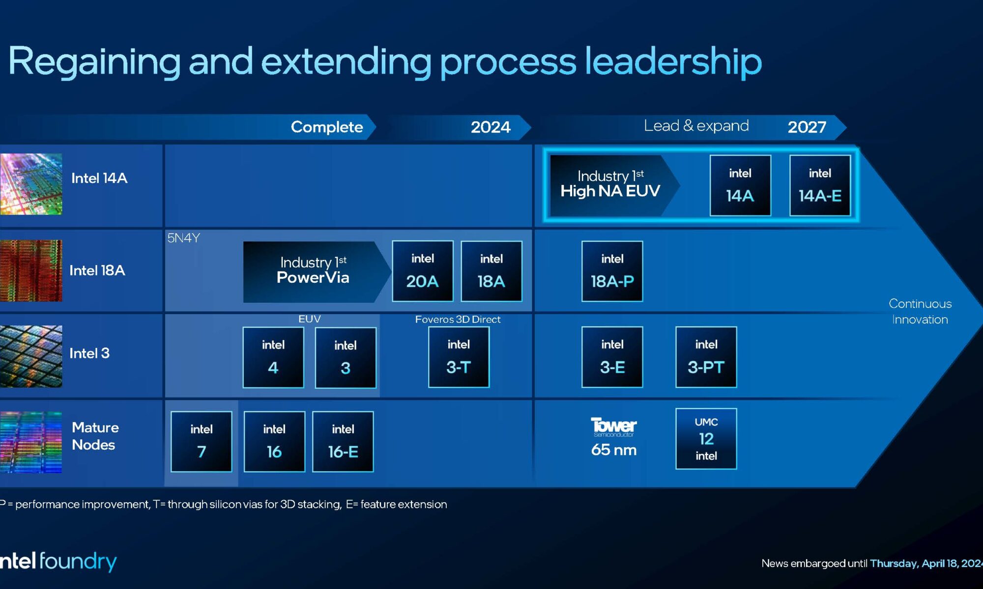
The 18A process is in development now and High NA is being developed for the future 14A process. Figure 1 illustrates Intel’s process roadmap.
 Page 07")
Figure 1. Intel Process Roadmap.
Over the history of the semiconductor industry there has been a continual drive to increase process density enabling more transistors in the same area. The first step in achieving more density is shrinking the lithographically printed features. Figure 2 illustrates the evolution of Exposure Systems and the resulting resolution.
 Page 10")
Figure 2. Exposure System Evolution.
In the lower left of figure 2 we can see the formula for the resolution of an optical system (Rayleigh’s criteria).
- CD is the critical dimensions, basically the smallest feature that can be resolved. Please note that the pitch achievable will be twice this number.
- K1 is a process related factor that generally ranges between 0.75 and 0.25 and typically gets smaller as the process matures (smaller k1 equals smaller feature size).
- λ is the wavelength of the exposing radiation. In the earliest exposure systems mercury arc lamps were used as a light source and G-line (436nm) and I-line (265nm) refer to peaks in the output spectrum of a mercury arc lamp. KrF (248nm) and ArF (193nm) refer to excimer lasers that combine Krypton (Kr) an inert gas and Fluorine (F) a reactive gas or Argon (Ar) an inert gas and F as a reactive gas in an excited state – in an excimer laser (excited dimer), these excited dimers decay giving off 248nm or 193nm light respectively. ArFi refers to ArF immersion (see NA below) and is also 193nm. EUV introduces a light source that uses a carbon dioxide laser to vaporize tin droplets producing 13.5nm light. As with k1 the smaller the wavelength the smaller the feature size that can be resolved.
- NA is the numerical aperture of the optics, a measure of the acceptance angle of the lens. Higher NA gathers more of the reflections and therefore more information/higher resolution. Higher NA systems generally require more complex optics and for large diameter lenses it is particularly difficult. The maximum NA that can be achieved in air is 1.0 and ArF dry systems at 0.93NA are the highest achieved in exposure systems. ArFi (ArF immersion) refers to the use of ultrapure water between the lens and the wafer and this enabled 1.35NA for ArFi systems versus ArF dry systems where exposure is done in air. The higher the NA the smaller the feature that can be resolved.
High NA is expected to simplify the process flow, provide better yield and more flexible design rules.
The first High NA tool prototype is at the ASML factory. Intel got the second High NA tool in January 2024, see figure 3.
 Page 08")
Figure 3. High NA System at Intel.
The system was shipped to Intel unintegrated and is being integrated only a few weeks behind the tool at ASML. The High NA tool (0.55NA versus 0.33NA for standard EUV tools) shares as many modules as possible with the 0.33NA tools, for example the laser source and wafer modules are the same as the new NXE:3800 0.33NA tool. The major development for the High NA tool is optics. There is a lot of data that the modules meet specifications and Intel as the first mover has a very close relationship with Zeiss (Zeiss builds the optics) and ASML. Mark said he is confident that the High NA tool will be available before there is too much multi-patterning required with 0.33NA tools.
Authors note, I asked if there was multi-patterning on the 18A process and he said there is some, not for resolution but for cutting to achieve tight tip-to-tip spacings.
Intel believes they are uniquely positioned to make the most of this tool with:
- Power via.
- Internal mask shop.
- Directed Self Assembly for defect repair.
- Using advanced illumination with advanced mask to push limits.
- Pattern shaping with directional etch (possibly Applied Materials Sculpta tool?).
The first light for a High NA tool has been achieved at the ASML factory and first light at Intel will be “soon”. Development of the 14A process using High NA is planned for 2025, Intel is doing some work on the tool at ASML to get a jump on development.
One consideration with the High NA tool is size and having a Cleanroom that can accommodate it. Figure 4 illustrates the relative sizes of Deep UV, EUV (0.33NA) and High NA EUV systems.

Figure 4. System Sizes.
From figure 4 we can see that the original 0.33NA EUV systems are dramatically larger than DUV systems, in fact, cleanrooms must be designed to accommodate EUV systems. If you go into a Fab with EUV systems, they are easy to spot because there is a crane above the tool for maintenance work. Intel for example has a lot of older fabs that can’t accommodate an EUV system without major modifications to the building structure. High NA systems are ever bigger than 0.33NA EUV systems. Interestingly Intel’s Fab D1X and Fab 42 were both designed to accommodate 450mm equipment and therefore should be High NA tool capable. All Intel’s new fabs just completed or being built would presumably be High NA capable.
The current High NA tools are NXE:5000 development systems, the production High NA tool will be the NXE:5200 and Mark mentioned there would be at least three more generations of High NA tools after the NXE:5200. With 14A planned to be production ready two years after 18A, that would imply Intel will need to start receiving NXE:5200 systems in 2026 and 2027.
There is some discussion of Hyper NA tools possibly with a NA of 0.75. Mark mentioned that a lot of what ASML developed for the 0.55NA tool can be used for 0.75NA and that the tool will be the same size as the 0.55NA tool. The potential application for the 0.75NA tool would be for interconnect but the economics haven’t been proven yet.
Another aspect of High NA is the anamorphic design with 4x reduction in one direction and 8x in the other. When you take the current 6” reticle, account for edge exclusion with 8x reduction the die size is constrained and for some large die, stitching may be required and that requires consideration of where on the die to stitch. Intel is pushing for new 6” x 12” masks as a productivity improvement to enable large die without stitching.
It wasn’t discussed on the call, but one key question would be how much of a benefit High NA is over 0.33NA. My detailed simulations of High NA EUV single exposure versus LESLE double exposure with 0.33NA EUV, yield a just over 10% cost reduction, this is in addition to cycle time, yield, and design rule advantages.
ASML recently announced they shipped the third High NA EUV system to an undisclosed customer, although there are rumors it went to TSMC. Intel has been the most vocal company about adoption of High NA, but it is clear at least one competitor is at evaluating it close on Intel’s heels.
Scotten Jones is President of Semiconductor Manufacturing Economics and a Senior Fellow at TechInsights. Stay up to date with the latest from TechInsights by accessing the Platform for free today. Register or Sign-in here.
Also Read:
No! TSMC does not Make 90% of Advanced Silicon
ISS 2024 – Logic 2034 – Technology, Economics, and Sustainability
Share this post via:


Comments
7 Replies to “Intel High NA Adoption”
You must register or log in to view/post comments.