You are currently viewing SemiWiki as a guest which gives you limited access to the site. To view blog comments and experience other SemiWiki features you must be a registered member. Registration is fast, simple, and absolutely free so please,
join our community today!
On Friday April 12th Intel held a press briefing on their adoption of High NA EUV with Intel fellow and director of lithography Mark Phillips.
In 1976 Intel built Fab 4 in Oregon, the first Intel fab outside of California. With the introduction of 300mm Oregon became the only development site for Intel with large manufacturing, development,… Read More
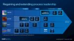
On Wednesday, February 21st Intel held their first Foundry Direct Connect event. The event had both public and NDA sessions, and I was in both. In this article I will summarize what I learned (that is not covered by NDA) about Intel’s business, process, and wafer fab plans (my focus is process technology and wafer fabs).
Business
…
Read More
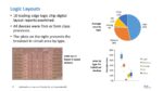
For the 2024 SEMI International Strategy Symposium I was challenged by members of the organizing committee to look at where logic will be in ten years from a technology, economics, and sustainability perspective. The following is a discussion of my presentation.
To understand logic, I believe it is useful to understand what makes… Read More
On May 22nd Applied Materials announced a new development center, Equipment and Process Innovation and Commercialization Center (EPIC).
Applied Materials already operates the Maydan Technology Center (MTC), a billion-dollar development facility with over 120 advanced process tools and 80 metrology and inspection tools… Read More
SEMICON West 2022 was held from July 12th to 14th at the Moscone Center in San Francisco.
On Monday the 11th before the show, Imec held a technology forum at the Marriott Marquee right around the corner from the Moscone center. In recent years the Imec forums have shifted away from the process technology I cover to more of a system and… Read More