For the 2024 SEMI International Strategy Symposium I was challenged by members of the organizing committee to look at where logic will be in ten years from a technology, economics, and sustainability perspective. The following is a discussion of my presentation.
To understand logic, I believe it is useful to understand what makes up leading edge logic devices. TechInsights produces detail footprint analysis reports, and I took reports for ten 7nm and 5nm class devices including Intel and AMD microprocessors, Apple A series and M series processors, an NVIDIA GPU, and other devices. Figure 1 illustrates what makes up the die area.
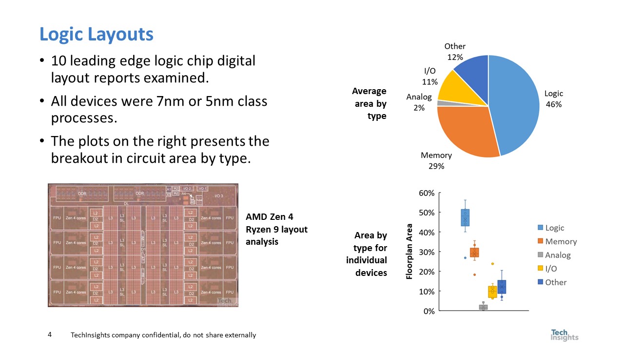
From figure 1 logic makes up slightly less than one half of the die area, memory slightly less that one third of the die and I/O, analog, and other the balance. I find it interesting that the SRAM memory areas actually measured is a lot smaller than the percentage I typically hear people talk about for System On a Chip (SOC) products. The plot on the bottom right shows that there is one outlier but otherwise the values are tightly clustered.
Singe logic makes up almost half the die area, it makes sense to start with the logic part of the design. Logic designs are done with standard cells and figure 2 is a plan view of a standard cell.
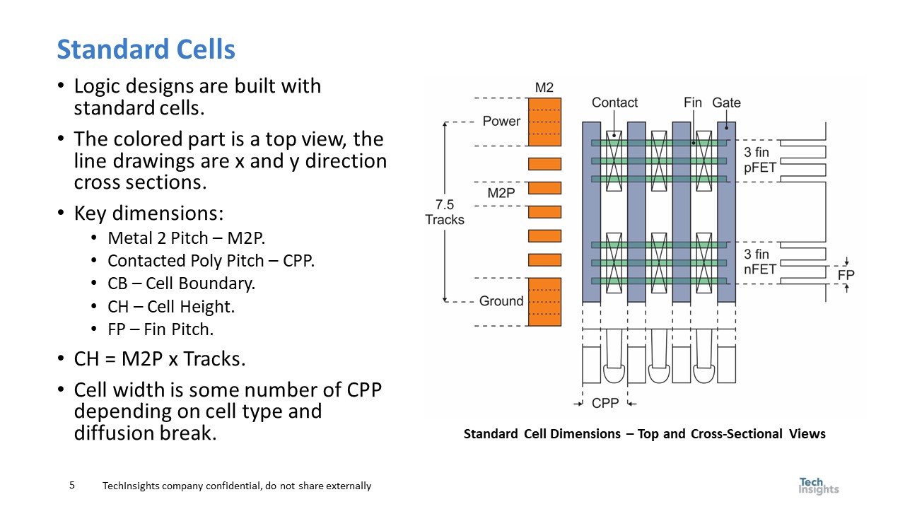
The height of a standard cell is typically characterized as the Metal 2 Pitch (M2P) multiplied by the number of tracks, but looking at the right side of the figure there is a cross sectional view of the device structure that must also match the cell height and is constrained by device physics. The same is the case for the cell width that depends on the Contacted Poly Pitch (CPP) and looking at the bottom of the figure there is a cross sectional view of the device structure that once again is constrained by physics.
Figure 3 presents the result of an analysis to determine the practical limits of cell width and cell height scaling. I have a presentation that details the scaling constraints and in that presentation there are dozens of slides between figure 2 and figure 3, but with limited time I could only show the conclusion.
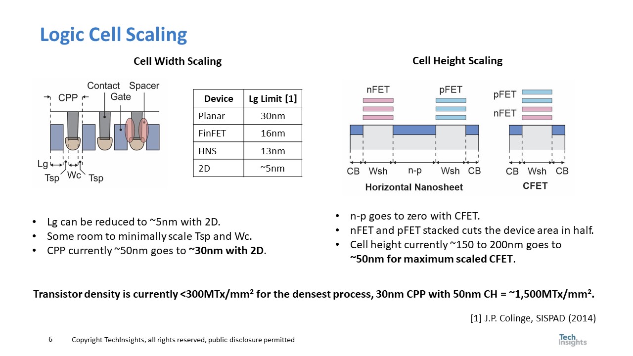
Cell width scaling depends on CPP, and the left side of the figure illustrates how CPP is made up of Gate Length (Lg), Contact Width (Wc) and two Contact to Gate Spacer Thicknesses (Tsp). Lg is constrained by leakage and the minimum Lg with acceptable leakage depends on the device type. Planar devices with a single gate controlling the surface of a channel with an unconstrained thickness, is limited to approximately 30nm. FinFETs and horizontal Nanosheets (HNS) constrain the channel thickness (~5nm) and have 3 and 4 gates respectively. Finally, 2D materials introduce <1nm channel thickness, non silicon materials and can produce Lg down to ~5nm. Both Wc and Tsp have limited ability to scale due to parasitics, The bottom line is a 2D device can likely produce a ~30nm CPP versus todays CPPs that are ~50nm.
Cell height scaling is illustrated on the right side of the figure. HNS offers single nanosheet stacks in place of multiple fins. Then the evolution to stacked devices with a CFET eliminates the horizontal n-p spacing and stacks the nFet and pFET. Cell heights that are currently 150nm to 200nm can be reduced to ~50nm.
The combination of CPP and Cell Height scaling can produce transistor densities of ~1,500 million transistor per millimeter squared (MTx/mm2) versus todays <300MTx/mm2. It should be noted that 2D materials is a likely a mid to late 2030 technology so 1,500 MTx/mm2 is outside of the timing discussed here.
Figure 4 presents a summary of announced processes from Intel, Samsung, and TSMC.
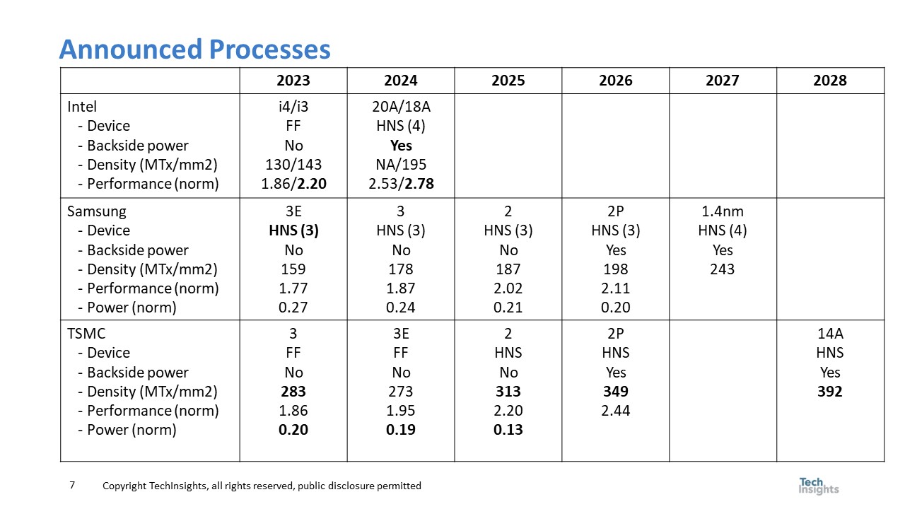
For each company and year, the device type, whether or not backside power is used, density, power and performance are displayed if available. Power and performance are relative metrics and power is not available for Intel.
In figure 4, leading performance and technology innovations are highlighted in bold. Samsung is the first to put HNS in production in 2023 where Intel won’t introduce HNS until 2024 and TSMC until 2025. Intel is the first to introduce backside power into production in 2024 and Samsung and TSMC won’t introduce it until 2026.
My analysis concludes Intel is the performance leader with i3 and maintains that status for the period illustrated, TSMC has the power lead (Intel data not available) and density leadership.
Figure 5 presents our logic roadmaps and includes projected SRAM cell sizes (more on this later).
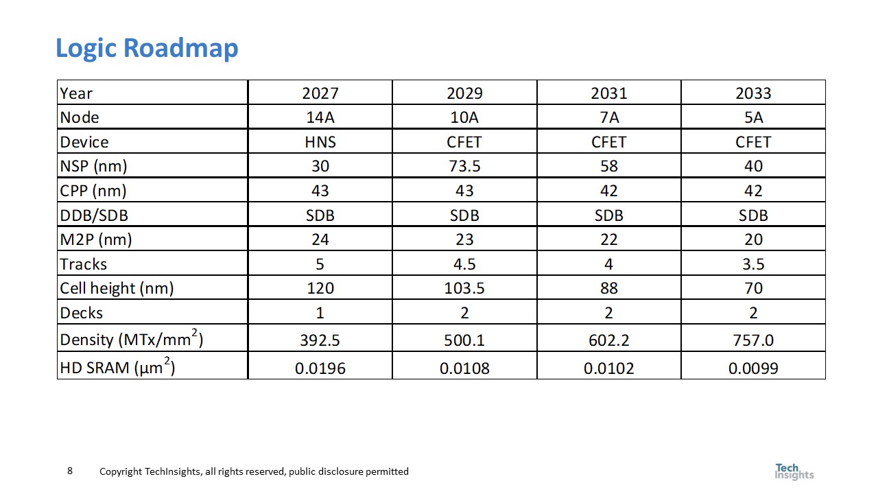
From figure 5 we expect CFETs to be introduced around 2029 providing a boost in logic density and also cutting SRAM cell sizes nearly in half (SRAM cell size scaling has virtually stopped at the leading edge). We expect logic density to reach ~757MTx/mm2 by 2034.
Both the logic transistor density projections and SRAM transistor density projections are illustrated in figure 6.
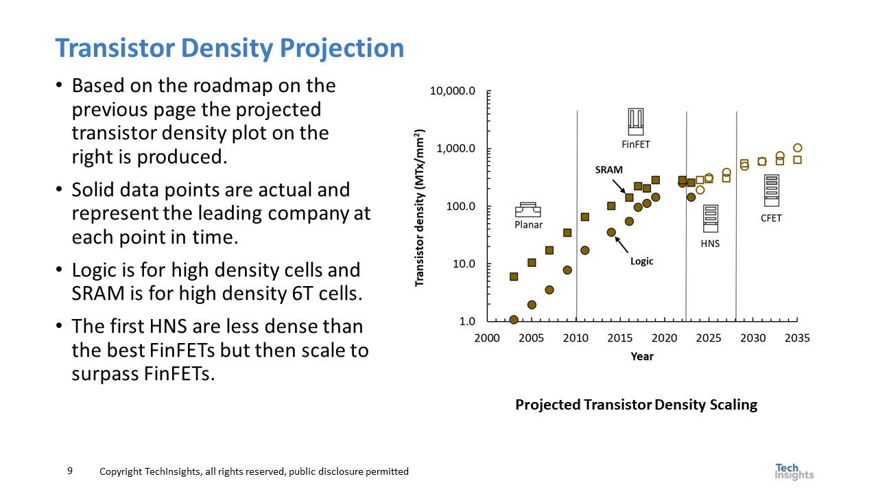
Both logic and SRAM transistor density scaling is slowing but SRAM to a greater extent and logic now has similar transistor density to SRAM.
Slide 7 summarizes TSMC data on analog scaling in comparison to Logic and SRAM. Analog and I/O scaling are both slower than logic scaling as well.
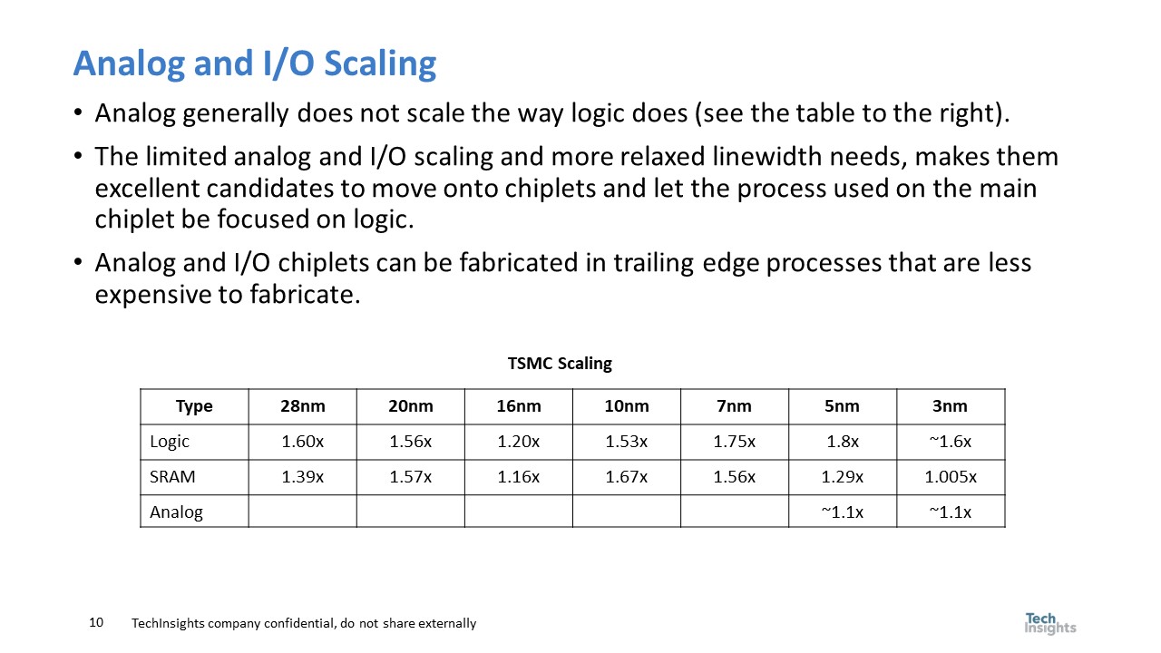
A possible solution to slower SRAM and analog and I/O scaling is chiplets. Chiplets can enable less expensive – more optimized processes to be utilized to make SRAM and I/O.
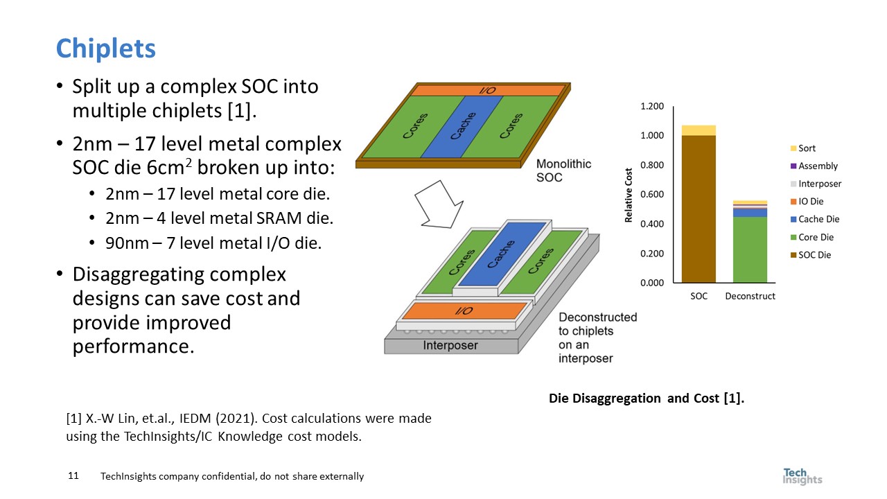
The figure on the right side of figure 8 comes from a 2021 paper I coauthored with Synopsys. Our conclusion was breaking apart a large SOC into chiplets could cut the cost in half even after accounting for increased packaging/assembly costs.
Figure 9 presents normalized wafer and transistor costs for logic, SRAM and I/O (please note the figure has been updated from the original presentation).
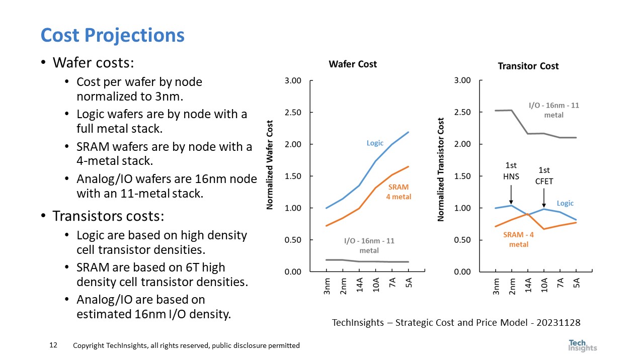
In the right figure the normalized wafer cost is shown. The logic wafer cost are for a full metal stack that is increasing in number of metals layers. The SRAM wafers are the same nodes but limited to 4 metals layers due to the more regular layout of SRAM. The I/O wafer cost is based on a 16nm – 11 metal process. I selected 16nm to get a minimum cost FinFET node to ensure adequate I/O performance.
The figure on the right is the wafer cost converted to transistor cost. Interestingly the I/O transistor are so large that even on a low cost 16nm wafer they have the highest cost (the I/O transistor size is based on TechInsights measurements of actual I/O transistors). Logic transistor costs go up at 2nm the first TSMC HNS sheet node where the shrink is modest. We expect the shrink at 14A to be larger as a second-generation HNS node (this is similar to what TSMC did with their first FinFET node). Once again, the cost of the first CFET node also increases transistor cost for one node. SRAM transistor cost trends upward due to limited shrink except for a one time CFET shrink. The bottom line of this analysis is that transistor cost reduction will be modest although Chiplets can provide a onetime benefit.
Moving on to sustainability, figure 10 explains the different “scopes” that make up carbon footprint.
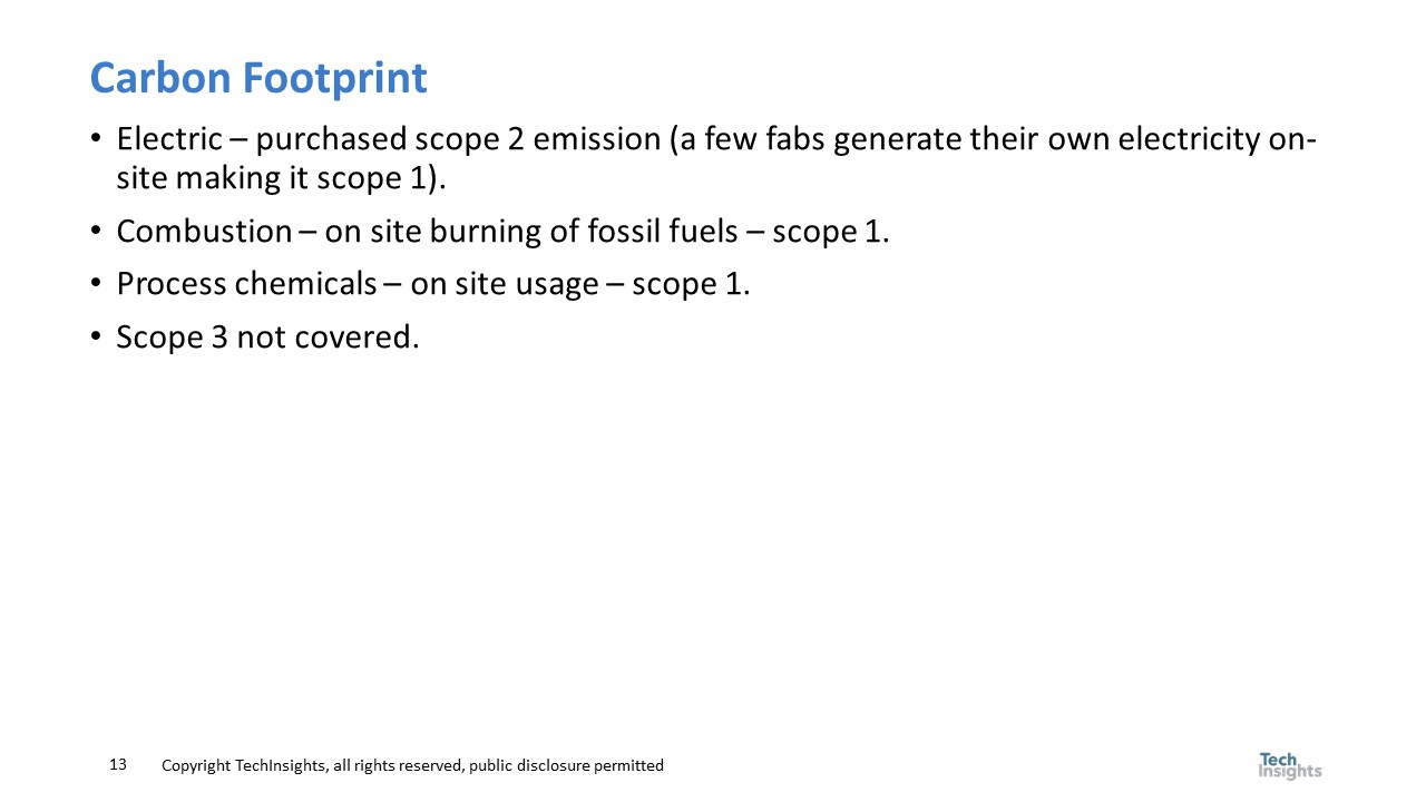
Scope 1 is the direct site emissions due to process chemicals and combustion (electric can also be scope 1 if generated on-site), Scope 2 is due to the carbon footprint of purchased electricity. Scope 3 is not included in this analysis but is due to the carbon footprint of purchased materials, the use of the manufactured product and things like vehicles driven by employees of a company.
A lot of companies in the semiconductor industry are claiming that they have no carbon emission due to electricity because the electricity is all renewable. Figure 11 compares renewable to carbon free.
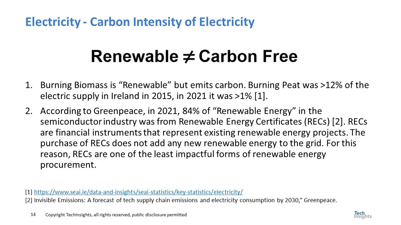
The key problem is that 84% of renewable energy in the semiconductor industry in 2021 was found by Greenpeace to be renewable energy certificates where a company purchases the rights to claim reductions someone else already did. This is not same as installing low carbon electric sources or paying others to provide low carbon electricity and does not in-fact lower the global carbon footprint.
Figure 12 illustrates how process chemical emissions take place and are characterized.
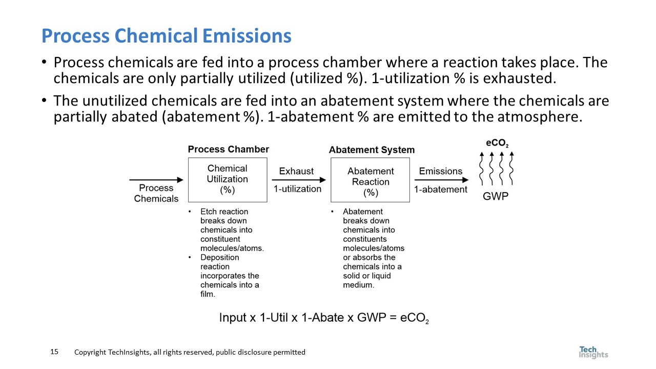
Process chemicals enter a process chamber where a percentage of the chemicals are utilized in an etching or deposition reaction that breaks down the chemicals or incorporates them into a deposited film. 1-uitlization is the amount of chemical that escapes out the exhaust of the tool. The tool exhaust then may go into an abatement chamber further breaks down a percentage of the chemicals and the emissions to the atmospheres from abatement are 1-abatement. Finally, a Global Warming Potential (GWP) is applied to calculate the carbon equivalency of the emission. GWP takes into account how long the chemical persists in the atmosphere and how much heat the chemical reflects back in comparison to carbon dioxide. Carbon dioxide has a GWP of 1, semiconductor process chemicals such as SF6 and NF3 have GWP values of 24,300 and 17,400 respectively (per IPCC AR6).
Figure 13 presents some options for reducing emissions.
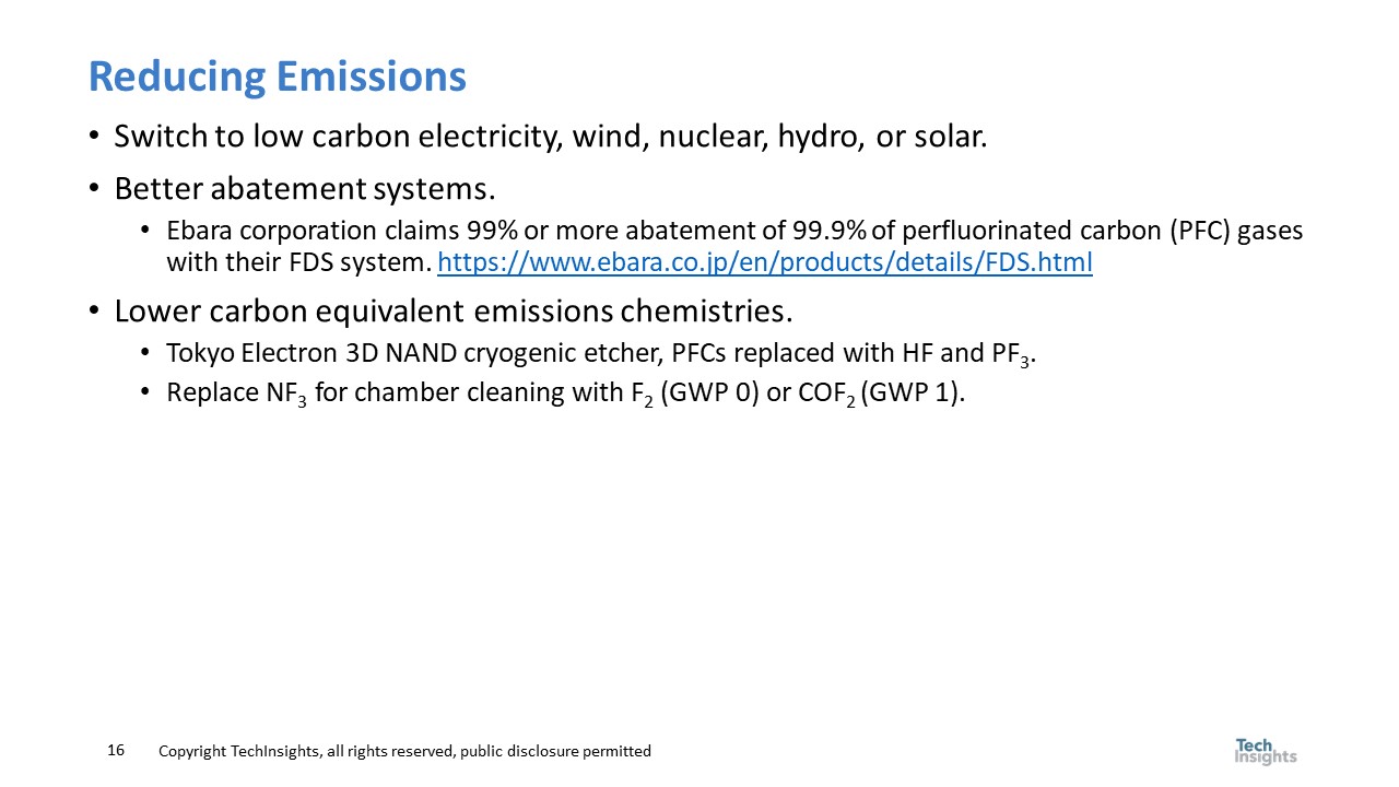
Electricity sources such as coal produce 820 grams of CO2 equivalent emissions per kilowatt hour (gCO2e/KWh) whereas solar, hydroelectric, wind, and nuclear power produce 48, 24, 12 and 12, gCO2e/KWh respectively.
More efficient abatement systems can breakdown process gases more effectively. Fab abatement system range in efficiency from 0% for some reported US sites (no abatement) to ~90%. We estimate the worldwide 300mm fabs average is ~70% and that most 200mm and smaller wafer size fabs have no abatement. Systems with up to 99% efficiency are available.
Lower emission chemistry can also be used. Tokyo Electron has announced a new etch tool for 3D NAND that uses gases with zero GWP. Gases such as SF6 and NF3 are primarily used to deliver Fluorine (F) into chambers for cleaning, substituting F2 (GWP 0) or COF2 (GWP 1) can essentially eliminate this source of emissions.
Figure 14 illustrates a Carbon Footprint Forecast for logic.
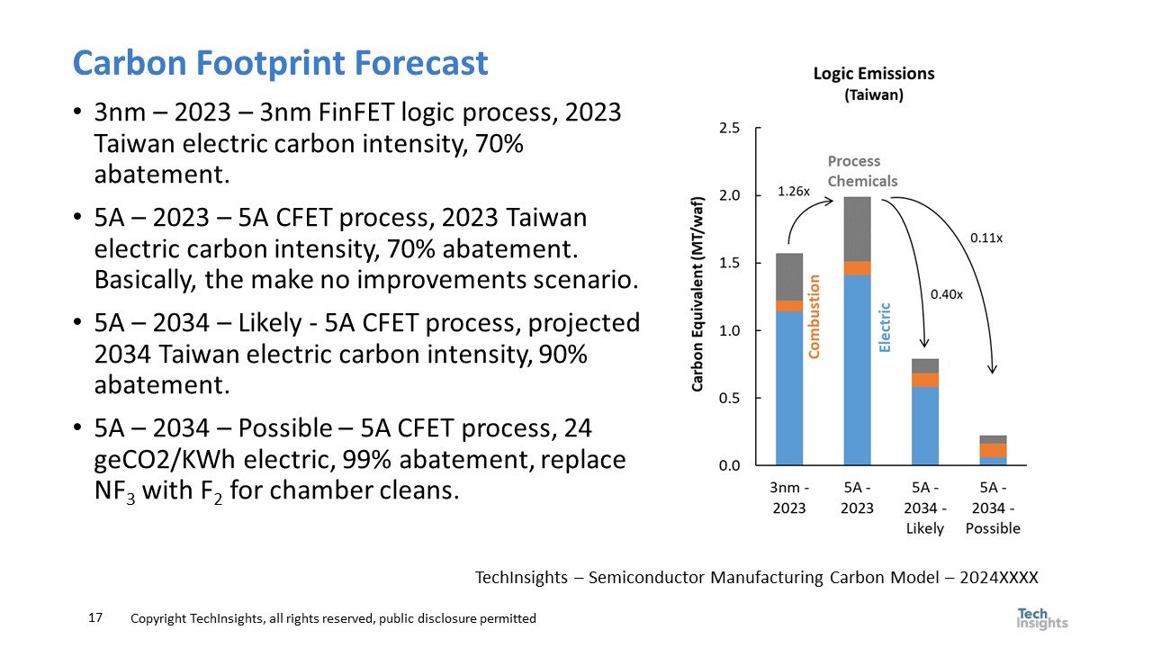
In the figure, the first bar on the left is a 3nm process run in Taiwan in 2023 assuming Taiwan’s electricity carbon footprint and 70% abatement. The second bar is a 5A process and the emission that would result if the same 2023 Taiwan electricity carbon intensity and 70% abatement were used. The increase in process complexity would drive up the overall footprint by 1.26x. Looking forward to 2034 Taiwan’s electricity is expected to decarbonize significantly, also 90% abatement should be common, and the third bar shows what a 5A process would look like under this condition. While this represents cutting emissions by more than half, growth in the number of wafers run by the industry for 2034 would likely overwhelm this improvement. The final bar on the right is what is possible with sufficient investment, it is based on low carbon electricity, 99% abatement, and using F2 for chamber cleaning.
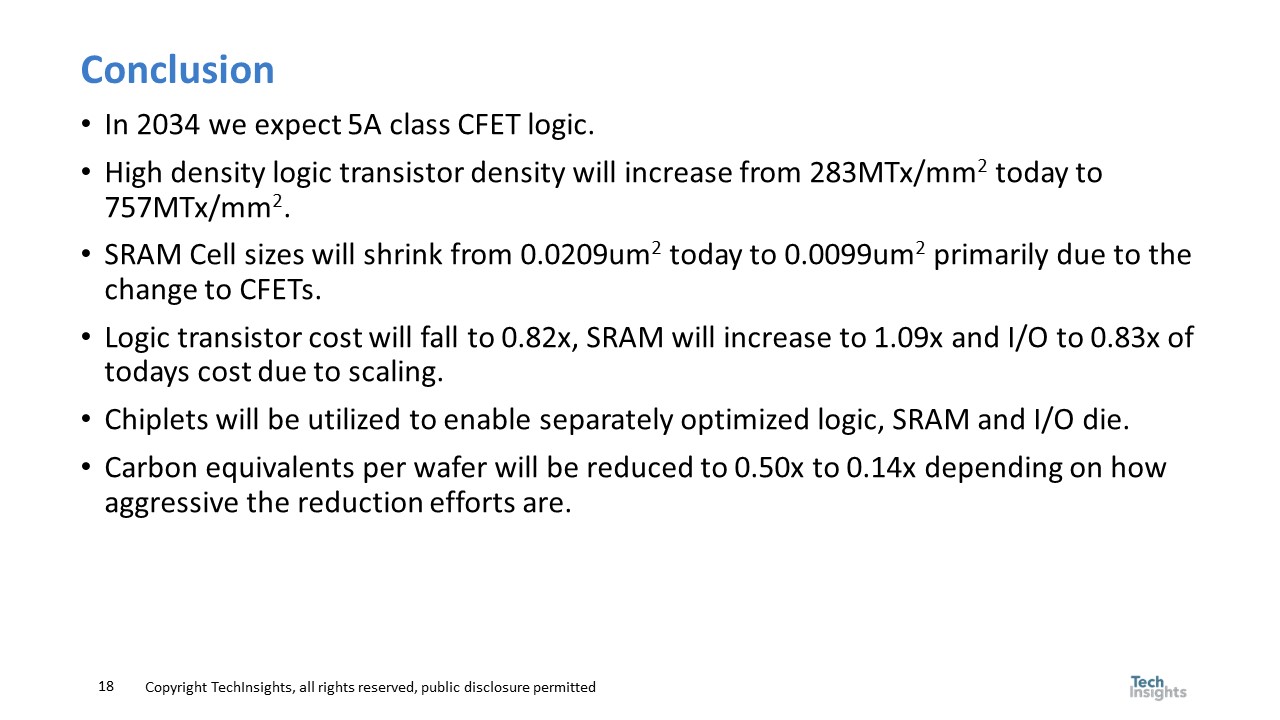
Figure 15 presents our conclusions:
Transistor density, and wafer and die cost estimates were generated using the TechInsights Strategic Cost and Price Model, an industry roadmap that produces cost and price estimates as well as detailed equipment and materials requirements. The GHG emission estimates were produced using the TechInsights Semiconductor Manufacturing Carbon Model. For more information, please contact sales@techinsights.com
I would like to acknowledge my colleagues in the Reverse Engineering Business Unit at TechInsights, their digital floorplan and process reports were very helpful in creating this presentation. Also, Alexandra Noguera at TechInsights for extracting I/O transistor sizing data for this work.
Also Read:
IEDM 2023 – Modeling 300mm Wafer Fab Carbon Emissions
SMIC N+2 in Huawei Mate Pro 60
Share this post via:


Comments
2 Replies to “ISS 2024 – Logic 2034 – Technology, Economics, and Sustainability”
You must register or log in to view/post comments.