
At IEDM 2023, Naoto Horiguchi presented on CFETs and Middle of Line integration. I had a chance to speak with Naoto about this work and this write up is based on his presentation at IEDM and our follow up discussion. I always enjoy talking to Naoto, he is one of the leaders in logic technology development, explains the technology in an easy-to-understand way and is responsive and easy to work with.
Why Do We Need CFETs
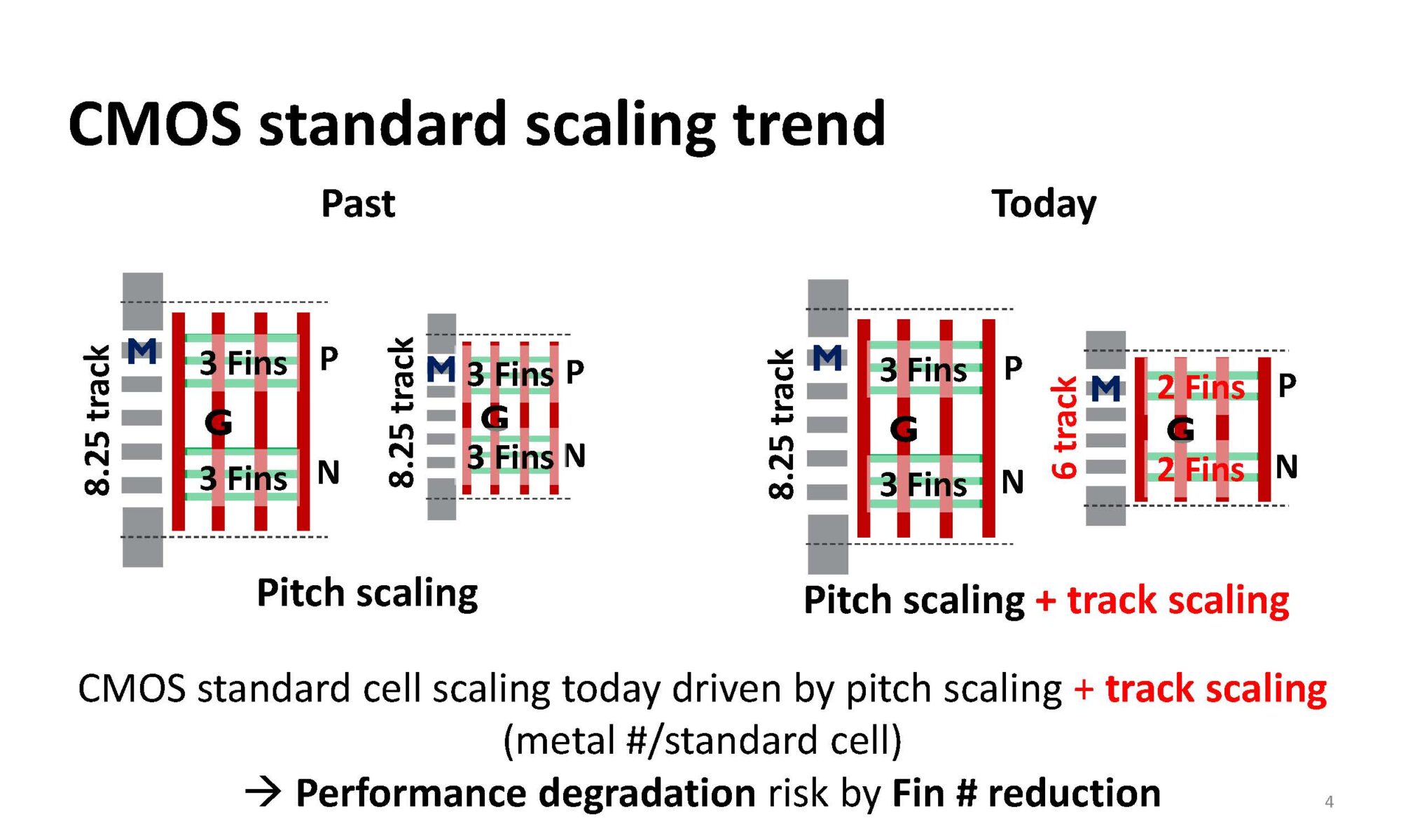
As CMOS scaling has transitioned from purely pitch based scaling to pitch plus track-based scaling, fin depopulation has become necessary, see figure 1. Each time you reduce the number of fins performance is reduced.

By moving from FinFEts to stacked Horizontal NanoSheets (HNS) performance can be improved/recovered by wider nanosheets stacks and stacking multiple nanosheets vertically, see figure 2.

But as we have seen with FinFETs nanosheet scaling eventually leads to reduced performance, see figure 3.

CFETs (Complementary FET) stack the nFET and pFET, see figure 4.

CFETs once again reset the scaling constraints because the nFET and pFET are stacked and the n-p spacing between the devices becomes vertical instead of horizontal, this enables wider sheets, see figure 5.

Figure 6 presents a comparison of HNS and CFET performance versus cell height highlighting the CFET advantage.

Monolithic Versus Sequential CFET
There are two fundamentally different approaches to CFET fabrication. In a monolithic flow the CFETs are fabricated on a wafer in a continuous process flow. In a sequential flow the bottom device is fabricated on one wafer, then a second wafer is bonded to the first wafer and the top device is fabricated in the second wafer.
In a sequential flow a bonding dielectric is present between the two devices, see figure 7.

Because of the bonding dielectric the structure is taller and has higher capacitance degrading performance, see figure 8.

Sequential CFETs are more expensive to fabricate than monolithic CFETs and between that and the performance degradation, it appears the industry is focused on monolithic CFETs.
Monolithic CFET Processing
The monolithic CFET process is illustrated in figure 9.

The steps in bold are particularly challenging:
- Horizontal Nanosheet Stacks (fins) are already high aspect ratio, then in order to make a CFET you stack the nFET and pFET stacks on top of each other with a relatively thick layer in between more than doubling the height.
- The gate formation is also high aspect ratio as described on the previous point.
- The epitaxial source/drains must be vertically isolated from each other.
- Not explicitly called out, the bottom device source/drain is fabricated and then the top device top source/drain is fabricated. The thermal processing of the top device and subsequent steps must be done at low enough temperatures to not degrade the bottom device.
One particularly interesting part of this presentation was the Middle Dielectric Isolation (MDI) part, I hadn’t seen this issue before. The MDI proves inner spacer and Work Function Material (WFM) patterning.
Figure 10 illustrates the MDI effect on inner spacer formation (left side) and WFM patterning (right side).

Figure 11 illustrates the MDI integration flow.

By integrating MDI the vertical spacing between the nFET and pFET can be increased without impacting the inner spacer formation.
As mentioned previously the bottom device source/drain is fabricated and then the top device source/drain is fabricated. After formation of the bottom source/drain, an isolation dielectric is deposited and etched back to expose the top device for source/drain epitaxial formation. The isolation etch back has to be controlled with the MDI height, see figure 12.

In order to minimize thermal degradation of device performance new WFM options with dipole first processing and no anneal and low temperature inter layer formation processes are needed, see figure 13.

Low temperature source/drain growth and low temperature silicides for contact formation are also needed, see figure 14.

The low temperature silicide will be particularly important for backside direct contact to the bottom device. CFET interconnect requires contacts to the bottom and top device and with the advent of backside power delivery the top device will be contacted from the front side interconnect stack and the bottom device will be contacted from the backside. Molybdenum (Mo) and Niobium (Nb) are promising for pFET and Scandium (Sc) is promising for the nFET, although Sc is hard to deposit with ALD.
Backside and Middle of Line Interconnect
As I have written about previously here Back Side Power Delivery Network (BSPDN) is expected to be introduce this year by Intel and by Samsung and TSMC in 2026. Splitting interconnect into frontside signal connections and backside power connections reduces IR drop (power loss) by an order of magnitude, see figure 15.

BSPDN also improves track scaling supporting a reduction from a 6-track to 5-track cell, see figure 16.

The integration of BSPDN with CFET can provide a 20% to 40% power reduction versus Horizontal stacked NanoSheets (HNS), see figure 17.

In order to go beyond a 5-track cell to a 4-track cell interconnect challenges must be overcome, see figure 18.

Vertical-Horizontal-Vertical layout with additional Middle of Line (MOL) layers can enable 4-track cells, see figure 19.

I have previously written about Imec’s work in this area here so I will not repeat that information.
I asked Naoto what it would take to go beyond a 4-track cell to a 3-track cell, he replied that Imec is working on that optimization now, that it may require addition MOL layers and possibly a top to bottom connection next to the device that would impact standard cell layout.
I also asked Naoto when he thought we might see CFETs implemented and he said possibly the A10 logic generation or A7 generation.
Authors note, Intel, Samsung, and TSMC all published work on CFETs at IEDM this year and both Intel and TSMC have technology option maps showing FinFETs giving way to HNS and then CFETs.
Conclusion
Imec continues to show excellent progress on the development of CFETs as a next generation option after HNS. In this work device integration options as well as BSPDN and MOL options have all been described.
Also Read:
IEDM 2023 – Modeling 300mm Wafer Fab Carbon Emissions
SMIC N+2 in Huawei Mate Pro 60
Share this post via:


Comments
6 Replies to “IEDM 2023 – Imec CFET”
You must register or log in to view/post comments.