imec announced that IC-Link by imec has joined the TSMC 3DFabric Alliance, a strategically important move that reflects the semiconductor industry’s transition from traditional monolithic scaling toward heterogeneous integration, chiplet architectures, and advanced packaging-driven system optimization. The partnership… Read More
Tag: imec
Crossing the Yield Cliff: IDP V6 and the Future of Manufacturing Forecasting
The paper, Industrial Defectivity Prediction (IDP) V6: A Two-Layer Yield Cliff Framework for Cross-Industry Mass-Production Forecasting, presents a generalized industrial yield-modeling architecture that extends the classical Negative Binomial framework through a two-layer phenomenological structure designed … Read More
Chemical Origins of Environmental Modifications to MOR Lithographic Chemistry
In the pursuit of advanced extreme ultraviolet (EUV) lithography for high-NA patterning, metal oxide resists (MORs) offer significant promise but face challenges like critical dimension (CD) variation due to atmospheric interactions. Presented at SPIE Advanced Lithography + Patterning 2025 by Kevin M. Dorney and colleagues… Read More
Beyond Moore’s Law: High NA EUV Lithography Redefines Advanced Chip Manufacturing
The imec installation of the ASML EXE:5200 High Numerical Aperture (High NA) extreme ultraviolet (EUV) lithography system at imec represents a pivotal advancement in semiconductor manufacturing and research. This system, installed in imec’s 300 mm cleanroom in Leuven, Belgium, introduces unprecedented lithographic resolution… Read More
Unraveling Dose Reduction in Metal Oxide Resists via Post-Exposure Bake Environment
In the realm of extreme ultraviolet (EUV) lithography, metal oxide resists (MORs) have emerged as promising candidates for advanced semiconductor patterning. However, their stability poses challenges, particularly interactions with clean-room environments like humidity and airborne molecular contaminants (AMCs) … Read More
imec on the Benefits of ASICs and How to Seize Them
In an era where product differentiation increasingly depends on performance, power efficiency, and form factor, Application-Specific Integrated Circuits (ASICs) have become the ultimate competitive weapon for innovative companies. Unlike off-the-shelf processors, FPGAs, or even ASSPs, a full- or semi-custom ASIC is… Read More
CMOS 2.0 is Advancing Semiconductor Scaling
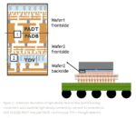
In the rapidly evolving landscape of semiconductor technology, imec’s recent breakthroughs in wafer-to-wafer hybrid bonding and backside connectivity are paving the way for CMOS 2.0, a paradigm shift in chip design. Introduced in 2024, CMOS 2.0 addresses the limitations of traditional CMOS scaling by partitioning… Read More
Exploring TSMC’s OIP Ecosystem Benefits
Now that the dust has settled let’s talk more about TSMC’s Open Innovation Platform. Launched in 2008, OIP represents a groundbreaking collaborative model in the semiconductor industry. Unlike IDMs that controlled the entire supply chain, OIP fosters an “open horizontal” ecosystem uniting TSMC… Read More
Rapidus, IBM, and the Billion-Dollar Silicon Sovereignty Bet
Can cash and IBM collaboration put Japan into premier-league chipmaking? Rapidus is betting billions it can.
When Japan announced the creation of Rapidus in 2022, the news was met with a mix of enthusiasm and skepticism. The company would enter the market at a time of escalating demand for semiconductor fabrication capacity to… Read More
Advancements in High-Density Front- and Backside Wafer Connectivity: Paving the Way for CMOS 2.0
In the rapidly evolving semiconductor landscape, imec’s recent breakthroughs in wafer-to-wafer hybrid bonding and backside technologies are reshaping the future of compute systems. As detailed in their article, these innovations transition CMOS 2.0 from a conceptual framework to practical reality, enabling denser,… Read More