
The SPIE Advanced Lithography Conference was held in February. I recently had the opportunity to interview Steven Scheer, vice president of advanced patterning process and materials at imec and review selected papers that imec presented.
I asked Steve what the overarching message was at SPIE this year, he said readiness for High NA is key. He identified three key ecosystem areas:
- Mask and Resolution Enhancement Technology (RET) infrastructure.
- Materials, photoresist and underlayers.
- Metrology
The exposure tools are also of course key, but that isn’t what Steve talks to. Authors note – I will be doing a write up on ASML’s SPIE presentations as well.
Masks
Steve went on to list out mask related issues:
- Mask 3d effects, such as focus shift and contrast loss – High NA is a low angle exposure making 3D effects more of an issue.
- Low defectivity mask blanks and masks with low variability in roughness and CD
- Low-n masks are needed to enable higher contrast and reduce mask 3D effects.
- Optical Proximity Correction techniques.
- Mask writing, multibeam.
- Mask stitching – the smaller size of the scanner field requires that die be stitched together.
- 4x one direction, 8x other direction requires a new type of mask design to enable stitching.
- Pellicles for higher source energy.
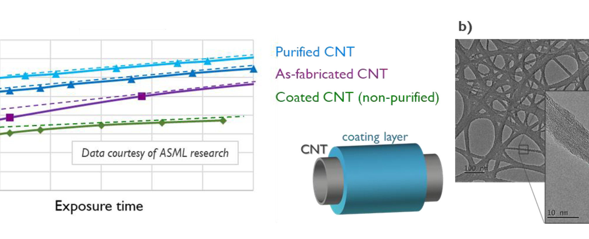
In “CNT pellicles: Recent optimization and exposure results,” Joost Bekaert et.al., explored Carbon Nanotube pellicles (CNT).
ASML has 600-watt source systems on their roadmap, current pellicles based on metal silicide are only viable up to approximately 400 watts. Pellicles need to block particles, have high transmission, sufficient mechanical strength to be suspended over an approximately 110mm by 140mm area, and be durable. CNT has showed up to 98% transmission. EUV radiation is so energetic that it creates a hydrogen plasma that etches the pellicle eventually leading to pellicle loss of mechanical integrity. imec has been evaluating etch rates and how to stabilize the pellicle.
Etch rates can be evaluated by looking at transmission, as the Pellicle is thinned by etching, transmission increases. Figure 1 illustrates the transmission over time of a Pellicle subject to various conditions.

ASML evaluates pellicle transmission versus exposure time utilizing an offline plasma exposure tool and in this work, imec demonstrated CNT pellicle exposure up to 3,000 wafers (96 dies at 30 mJ/cm² per wafer), and showed correlation between the results obtained from actual scanner exposure and those from the offline tool.
Pellicles initially have volatile organic impurities from the manufacturing process that absorb EUV energy until they burn off, see the green and purple curves. Baking the Pellicle at high temperatures “purifies” the pellicle by burning off the contaminants resulting in etch rate dominated transmission changes. The slope of the two blue curves is due to the etch rate. The green curve illustrates a “coated” pellicle that exhibits a lower etch rate, however the coating reduces transmission and may not be compatible with very high-power levels.
Photoresist
Steve, then discussed photoresist.
For photoresist a 24nm to 20nm pitch is a sweet spot for High NA insertion with 16nm pitch the ultimate resolution. Chemically Amplified Resist (CAR) has poor performance below 24nm. Metal Oxide Resists (MOR) look promising down to 17nm or even 16nm. Defectivity is still an issue. Doses at for a 24nm pitch is 67mJ/cm2 for MOR and 77mJ/cm2 for CAR. MOR has some stability issues and the lower the dose the more reactive/less stable the resist is. These are challenges, not showstoppers.
In “Scaled down deposited underlayers for EUV lithography,” Gupta et.al., explored photoresist underlayers. As pitch is shrunk, for the same photoresist layer the aspect ratio increases and can lead to pattern collapse. Improved underlayer adhesion can address this. Alternately a thinner photoresist can be utilized to manage aspect ratio but this can lead to etch issues unless a high etch selectivity under layer can be found.
imec found that surface energy of deposited underlayers can be matched to the photoresist to achieve improved adhesions. Density tuning of the deposited underlayer can be utilized to provide improved etch selectivity.
In “Dry Resist Patterning Readiness Towards High NA EUV Lithography,” Hyo Sean Suh et.al., from imec and Lam explored Lam’s dry photoresist process. For N2+ and A14 processes Metal 2 pitch (M2P) is expected to be ~24nm with 15nm tip-to-tip (T2T) and then at A10 M2P will be ~22nm with <15nm T2T.
The Lam dry resist process is illustrated in figure 2.

Post Exposure Bake (PEB) was found to strongly drive dose reduction but affected bridges and roughness. Co-optimizing development and etch mitigates bridges and roughness and showed a robust process window for 24nm pitch L/S patterning.
In “Feasibility of logic metal scaling with 0.55NA EUV single patterning,” Dongbo Xu et.al. described an evaluation of what High-NA (0.55NA) system can achieve with single patterning.
They concluded that 24nm pitch looks achievable. 20nm looks promising in the horizontal direction but the vertical direction needs more work. 18nm pitch needs additional work.
EUV has proven to be a very challenging technology from a Line roughness and stochastic defect perspective. Directed Self Assembly (DSA) is a technology that has been around for a long time but hasn’t gotten much traction. DSA is now getting attention as a technique to address line roughness and stochastic defects for EUV.
In “EUV LITHOGRAPHY LINE SPACE PATTERN RECTIFICATION USING BLOCK COPOLYMER DIRECTED SELF ASSEMBLY: A roughness and defectivity study,” Julie Van Bel et.al. found that combining DSA with EUV is superior to DSA processes based on Immersion lithography with lower line width roughness and no dislocation defects.
In “Mitigating Stochastics in EUV Lithography by Directed Self-Assembly,” Lander Verstraete et.al. explored using DSA to mitigate stochastic defects in EUV processing.
The imec process to rectify line/space EUV defects is illustrated in figure 3.

The imec process to rectify defects in contact arrays is illustrated in figure 4.

EUV plus DSA looks very promising for line/spaces at a 28nm pitch with the primary defect being bridges. At a 24nm pitch improvement is needed with too many bridge defects. Defects correlate with the block copolymer formulation and anneal time.
For contact arrays EUV + DSA improves Local Critical Dimension Uniformity (LCDU) and Pattern Placement Error and enables a lower dose.
Metrology
As film thicknesses are reduced metrology signal to noise ratios become a problem.
With EUV there is a defectivity process window, on one side there is a cliff where breaks in the pattern become an issue and on the other side of the windows there is a cliff where bridges between patterns become a problem.
When a new pitch is attempted there are a lot of defects that are driven down over time.
It is hard to measure a large enough area with sufficient sensitivity. E beam inspection is sensitive but slow, optical is fast but not sensitive. New 3D processes like CFET introduces additional challenges.
In “Dry Resist Metrology Readiness for High NA EUVL,” Gian Francesco Lorusso et.al, investigate Atomic Force Microscope (AFM), E Beam inspection and CD SEM for characterization of very thin photoresists.
Using the Lam dry photoresist process< CD SEM was shown to be viable down to 5nm thick photoresist. As resist thickness decreased line roughness increased, printability of bridge defects decreased while break defects remained the same. Pattern collapse was only seen in thicker films. AFM measurements indicated film thickness decreases. E Beam showed good capture of defects even for very thing films.
In “Semiconductor metrology for the 3D era,” J. Bogdanowicz et.al., explore the challenges of metrology on 3D structures.
In the 3D era, the Z direction has become the new X/Y scaling. For logic devices, CFET and Semi damascene presents challenges, in memory 3D DRAM is a future challenge, and 3D interconnects for System Technology Co Optimization (STCO) are another challenge.
For Horizontal Nanosheet and CFET processes lateral recess and fill characterization and detecting residues and other defects in multilayer stacks will be critical. In 3D Memory high aspect ratio (HAR) hole/split profiling and similar to logic detecting buried defects and residues in multi layers films will be critical. For STCO applications integrity of bonding interfaces and alignment will be key.
For traditional surface metrology there is already a trade off between sensitivity and speed, now inspection depth versus lateral resolution is a key trade off. Figure 5 presents the probing depth versus lateral resolution and throughput for various metrology techniques.

Figure 6 summarizes the current readiness of 3D metrology to address various needs.

From figure 6 there are still a lot of challenges to overcome to achieve a comprehensive metrology program.
Conclusion
The era of High NA EUV is approaching. There is good progress being made in pellicles, photoresists, and metrology and imec continues to work in all three areas for further progress.
Also Read:
TSMC has spent a lot more money on 300mm than you think
SPIE Advanced Lithography Conference 2023 – AMAT Sculpta® Announcement
IEDM 2023 – 2D Materials – Intel and TSMC
Share this post via:


Comments
There are no comments yet.
You must register or log in to view/post comments.