At #61DAC our very own Daniel Nenni from SemiWiki moderated an informative panel discussion on the topic of 3D IC Design Ecosystem. Panelists included: Deepak Kulkarni – AMD, Lalitha Immaneni – Intel Foundry, Trupti Deshpande – Qualcomm, Rob Aitken – CHIPS, Puneet Gupta – UCLA, Dragomir Milojevic – imec. Each panelist had a brief opening statement, then Daniel guided them through a series of questions, so I’ll paraphrase what I learned.
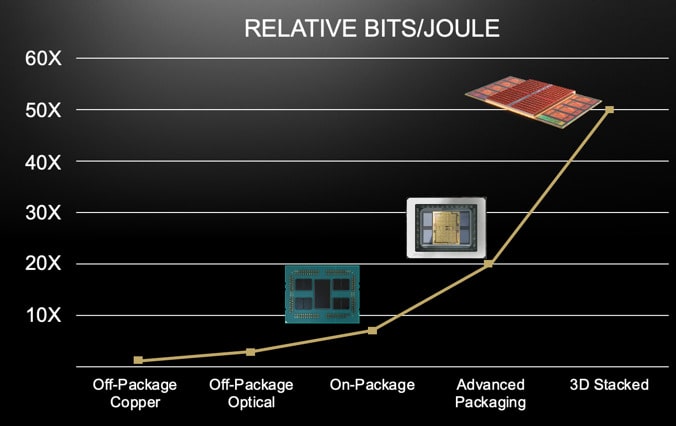
Deepak Kulkarni, AMD – there are big challenges in AI and the data centers caused by power consumption, because it’s taking megawatts to train a model with a trillion parameters over 30 days, and power projections of 100MW to train 100 trillion parameters.
For 3.5D packaging the motivation is improved power efficiency, where 3D Hybrid bonding has the densest and most power-efficient chiplet interconnect. Using 2.5D helps package HBM and compute together, and the goal is better system-level efficiency.
Lalitha Immaneni, Intel Foundry – We’re taking a systems approach to integrating 3D IC products and architected the first Chiplets at Intel, we want to move to a CAD agnostic tool flow. To improve our architecture, we need System Technology Co-Optimization (STCO), allowing all of the silicon-package-board trade-offs, so this is a multi-disciplinary task. We are combining key partners in industry and academia to collaborate, then we will pick the best point tools with data flowing through them, and we need a digital twin to help optimize our goals.
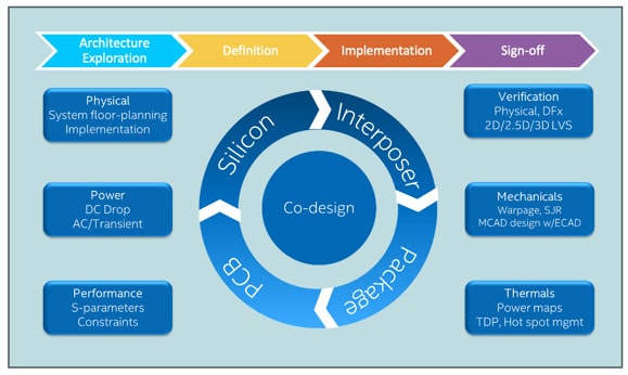
Trupti Deshpande, Qualcomm – How do I co-optimize and shift-left? Through early analysis, and we want to use the best tools, and stay EDA vendor-agnostic, to tackle this multi-physics challenge.
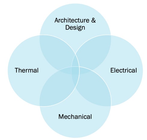
Rob Aitken, CHIPS – recently joined and came from Synopsys. 3D stacked die is inevitable, just look at the analogy to cities as they are similar to IC challenges. The transportation bottleneck at Moscone is the escalators. 3D Stacked die has similar challenges, vertical and thermal issues, new EDA requirements, and the bandwidth requirements are going up, so how do we solve all these challenges simultaneously?
Punnet Gupta, UC Los Angeles – Where are the system bottlenecks, hardware or software?
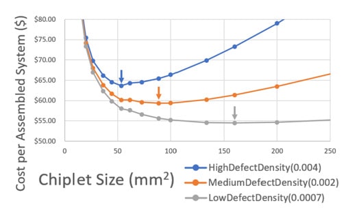
Software improvements can sometimes be larger than hardware improvements. We expect chiplets to be the next IP approach, and the chiplets must be large enough to be practical. Right now, the average chiplet is about 100mm2 to be economically feasible, so not tiny sizes.
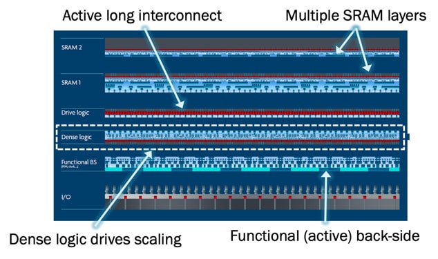
Dragomir Milojevic, IMEC – Looking at the scaling roadmap for CMOS it is slowing down, so multi-layered ICs are the future, let’s call it CMOS 2.0, where STCO is the new challenge.
Q&A
Q: How do you make the connections between 3D IC layers?
Dragomir – It’s with layer-to-layer wires, not monolithic wires.
Q: What is the motivation for Chiplets? AMD and Intel have had Chiplets for 7 years. For 3DIC what is the best method?
Rob –It’s the pressure from AI accelerators that drives these approaches, and monolithic chips are reticle size limited. 3D stacking of memory on logic is the easiest place to start. The 3D pressure is relentless, as the reward is so great.
Q: Dan – when did Arm start stacking?
Rob – In the mid-2000s there was a project started at Arm, but soon killed by the CTO.
Dragomir – The early benefits were not cost effective for stacking ICs.
Deepak – The motivations are economic and also the2X performance goals, no other solutions are out there.
Lalitha – We’ve been using traditional organic packages, then HBM, and now new substrates, as HPC and AI segments require new approaches.
Punnet – 3D helps you to get smaller areas for more cost-effective designs
Trupti – Mobile requires a good ROI to be pursued as an approach.
Rob – Airplanes require a retrofit to fit new equipment into the existing cabinet space, so less cost constrained approaches are welcomed.
Q: Dan – TSMC entered packaging 15 years ago, and Intel has also opened their packaging to customers. How will this work out?
Rob – The new packaging technology advances inside of IDM companies and the foundries.
Lalitha – There’s no limit to bridges added for EMIB by Intel Foundry, and it’s a huge differentiator.
Q: Dan – How heat will be dealt with?
Dragomir – We’ve done lots of experiments on multi-die stacking, and it’s not as bad as you may think. The speed of circuits dictates both power and thermal, so slowing speeds achieves thermal requirements.
Lalitha – We need to work with material science, heat spreaders, and new thermal cooling technology. There must be an architecture for co-optimization, where we find hot spots in each tile layer, then keep the hot spots apart, requiring a thermal-aware tool flow.
Rob – Through architecting, planning, designing, monitor it while it’s running for thermal, and then tune the voltage to keep thermal within limits.
Puneet – Even photonic circuits are quite sensitive to thermal coupling.
Q: What does an AI accelerator designer need to think about for 3D IC?
Trupti – They need to look at the entire system, not just the pieces, so the power per chiplet, then identify bottlenecks, and even considering mechanical aspects.
Rob – We’re in the early stages of 3D IC design, so we’re not so sure, eventually we will settle on a methodology, say in 10 years.
Lalitha – The boundaries between IC, package and board will merge with co-optimization. Tiles share the same package and substrate, and adding more tiles will add warpage. Silicon to package to platform all need to be co-designed. Better planning makes this process OK.
Deepak – What do I want with my AI accelerator? I want to double compute and double memory every two years to meet my requirements. Bringing compute and memory closer together helps to keep me within the power budget. Networks used to have 10% in data center power, but now its grown to 20%.
Q: Dan – How is power delivery from board to substrate to stack?
Puneet – Yes, power delivery is challenging, and requires backside power delivery in the stack. For thermal reasons, I want my highest power die to be at the top of stack. For delivery, I want highest power to be at the bottom of the stack.
Deepak – The total power delivered to a data center is our goal for reductions. Power at the data center is fixed, so how to get efficient enough through 3D stacking is the challenge.
Dragomir -Backside power delivery is required.
Q: Dan – What is backside power delivery?
Rob – Transistors with metal layers on top have to reach the lower layers. So, backside power comes from the other direction, the bottom of the die.
Dragomir – By putting PDN on the backside it then frees up the top side for interconnect.
Q: Dan – Where is EDA at now to support 3DIC?
Lalitha – The 3D design complexity is growing, so EDA vendors have responded, and we need early estimates from EDA planning tools in the presence of few initial details. We want a lightweight STCO tool for early estimates, then we want to choose multiple vendor tools using agnostic tools.
Q: Dan – The backside power has worse thermal issues for signals on topside routing. How should that be dealt with?
Rob – Yes, there are unintended consequences to backside power. My question is how does it work for EDA vendors to interoperate for 3DIC design flows?
Lalitha – It does work to be EDA agnostic.
Q: Dan – EDA tool companies have full-breadth flows, so how do they make their tools interoperate with competitors?
Deepak – The trend is more package-oriented EDA tools, so we still have to piece together and EDA flow for 3D IC.
Puneet – Don’t break an IP block into multiple layers.
Q: Dan – Every stage needs to change for 3DIC in your EDA tool flows, starting at design entry stages. Are the packages going to segregate into hot and cool regions? What about liquid cooling inside the package?
Deepak – Yes, cooling is an active research area.
Rob – The Aurora machine has power entering one side and a fire hose for cooling on the other side, so yes, liquid cooling makes sense.
Q: Dan – Will there be 200nm pitch used in packages?
Dragomir – Yes, dense interconnects between package layers is coming.
Puneet – The dimensions of pitches in packages are not changing that rapidly.
Rob – With a 200nm pitch it creates challenges for alignment, etc. Existing 3D stacks use memory bandwidths in small areas to maintain active high density, and high yield.
Deepak – 3D stacks more than two dies are limited by TSV interconnects. Two dies face to face are easier to accomplish.
Q: Dan – what about AI and ML trends, are they effecting your jobs today? Any co-pilot tools?
Trupti – We’re not seen many AI/ML tools for our jobs, but maybe a design of experiments would help us out on placement options.
Dragomir – We’re not using AI in STCO today yet for exploration.
Q: Dan – haven’t we been using ML in simulations?
Deepak – Yes, some AI/ML is used during the design phase, but not sign-off stages much yet.
Lalitha – AI/ML can help out in 3D IC testing.
Rob – There are EDA tools with AI/ML now, like for test.
Audience – Siemens has AI/ML in test tools now.
Rob – 10 years ago for image detection problems, the 1’s and 0’s in a test looked like an image, so AI can work for reducing that problem. Make your EDA problem look like something that AI/ML can solve.
Audience – Are my AI/ML results valid and accurate?
Rob – In the 80s we had Expert systems, but they weren’t AI. Is ML really AI?
Puneet – Where is the low-hanging fruit for generative AI? EDA tool documentation is quite poor, so why not use generative AI for documentation, like Copilot.
Q: Dan – What is the future of SoC designs?
Dragomir – On chip optical is one direction, having multiple layers.
Puneet – My optics colleagues say that Terabits/second on a single lane is coming.
Rob – Photonics is an obvious approach for longer distances, while shorter distances are going to use vertical metal connections.
Trupti – It’s the ROI that drives our choices, so academia needs to invent something optical that is cheap and reliable, then we will use it.
Lalitha – Optics still has a way to go.
Deepak – Sooner or later photonics will be used, but the costs are the main issue, pJ/bit is the driver.
Q: Dan – co-optimization and design exploration, what can you do well today? What do you really want to do soon?
Trupti – A lightweight system is wanted for multi-physics exploration, how thermal/power/warpage are co-optimized. Four or five area optimization is what’s really wanted.
Lalitha – We work with Cadence, Siemens and Synopsys on co-optimization for 3DIC, so it is progressing.
Rob – DTCO is working well today, as everyone is talking together, and the decisions per domain are now answered across domains.
Q: Dan – what is the role of standards today, like UCIe?
Lalitha – New standards are critical, and we should learn from the motherboard vendors. Chiplets across different process nodes are not standardized, it’s all manual. The utopia of mixing and matching chiplets will help, so the UCIe spec has all the details in it for a new standard.
Deepak – Standards are critical for Chiplets in UCIe. The shortcoming is more than die to die, so getting out of chiplet is important too.
Rob – Standards come from committees and take too much time, or there are Defacto standards. Most success is through Defacto standards. Existence proofs are much better than committees.
Lalitha – Let’s come up with a test case to help drive standards.
Puneet – New standards need to have open access for free sharing of information, like OpenAccess being free to use.
Q: Dan – What about 3D IC yield?
Dragomir – In research we have come up with ideas and solutions, but not a focus on the cost of 3DIC. Some cost models are built for 3DIC, taking into account yields.
Puneet – Yield and cost are tied closely to test, and the known good die problems, so it all depends on how each layer is tested, but it’s still an open question.
Q: Dan – What are the drivers for the semiconductor industry today? Is it AI?
Dragomir – Smart phones have been drivers for awhile. Many different segments are driving, like medical.
Puneet – AI is a big driver for advanced packaging today.
Rob – AI is driving semiconductor per TSMC (50% HPC and Mobile, both AI-driven).
Trupti – It’s mostly AI and mobile as the semi drivers, along with IoT, driving advanced packaging.
Deepak – AI for data centers and the accelerator market.
Q: Dan – Any comment on timelines for these advancements?
Dragomir – Hybrid bonding and stacking are done technologies. Within one year we will see things better, like DTCO and STCO.
Puneet – 3DIC for low-cost is something we haven’t discussed yet, as we are very focused on the data center today.
Rob – What was leading edge 15 years ago? 45nm. Now, that’s low-end, a mature technology.
Lalitha – EMIB package design kits are available now, and the EDA vendors are using this now. Co-optics and glass substrates are coming. STCO is analysis paralysis for now.
Deepak – Chiplet growth is driving fast, so expect more advanced packaging coming.
Q: Dan – What about sustainability, carbon footprints, dumping old electronics, how will this change the lifecycle?
Dragomir – It used to be that every iPhone lasted 4-5 years, but children’s phones last shorter, so we need more education of consumers for recycling.
Puneet – 3DIC shrinks the footprint for recycling, but there’s no repairability.
Trupti – How about energy efficiency, like for a server farm? Look at energy efficiency goals
Rob – Dumping heat into the atmosphere should be priced and taxed somehow.
Summary
It’s kind of rare that a group of panelists from the semiconductor industry, academia, design, government and research assemble together, but this group at DAC certainly took on the challenges of the emerging 3D IC design ecosystem. There were plenty of questions raised and answered about the current state of the 3D design environment, and the future directions being pursued.
Audience members were actively engaged and asked good questions, even the panelists raised their own questions to get feedback. I was typing at maximum speed to catch the gist of the conversations, and learned much from this gathering.
Related Blogs
Share this post via:


Comments
One Reply to “3D IC Design Ecosystem Panel at #61DAC”
You must register or log in to view/post comments.