At the 2023 VLSI Symposium on Technology and Circuits, Intel presented two papers on their PowerVia technology. We received a pre-conference briefing on the technology embargoed until the conference began and received the papers.
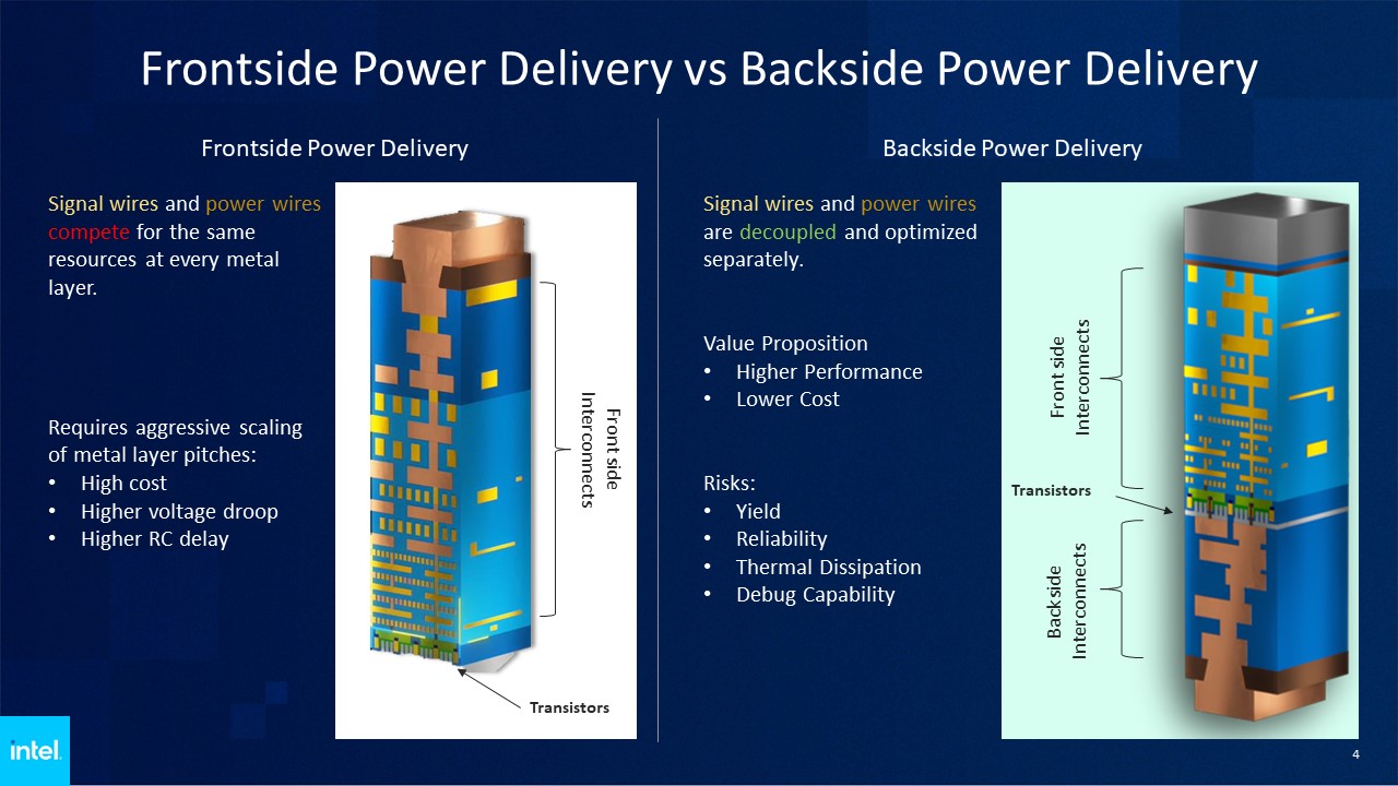
Traditionally all interconnects have taken place on the front side of devices with signal and power interconnects sharing the same set of interconnect layers. There is a fundamental trade off between signal routing where small cross sectional area routing lines are required for scaling and large cross sectional area routing lines are needed for low resistance/power drop power delivery. Moving power delivery to the backside of a wafer, Backside Power Delivery Network (BS-PDN) enables optimized signal routing layers on the frontside and optimized power delivery layers on the backside with big/thick power interconnects, see figure 1.
As logic technology has advanced the number of interconnect layers required has been steadily growing, see figure 2.
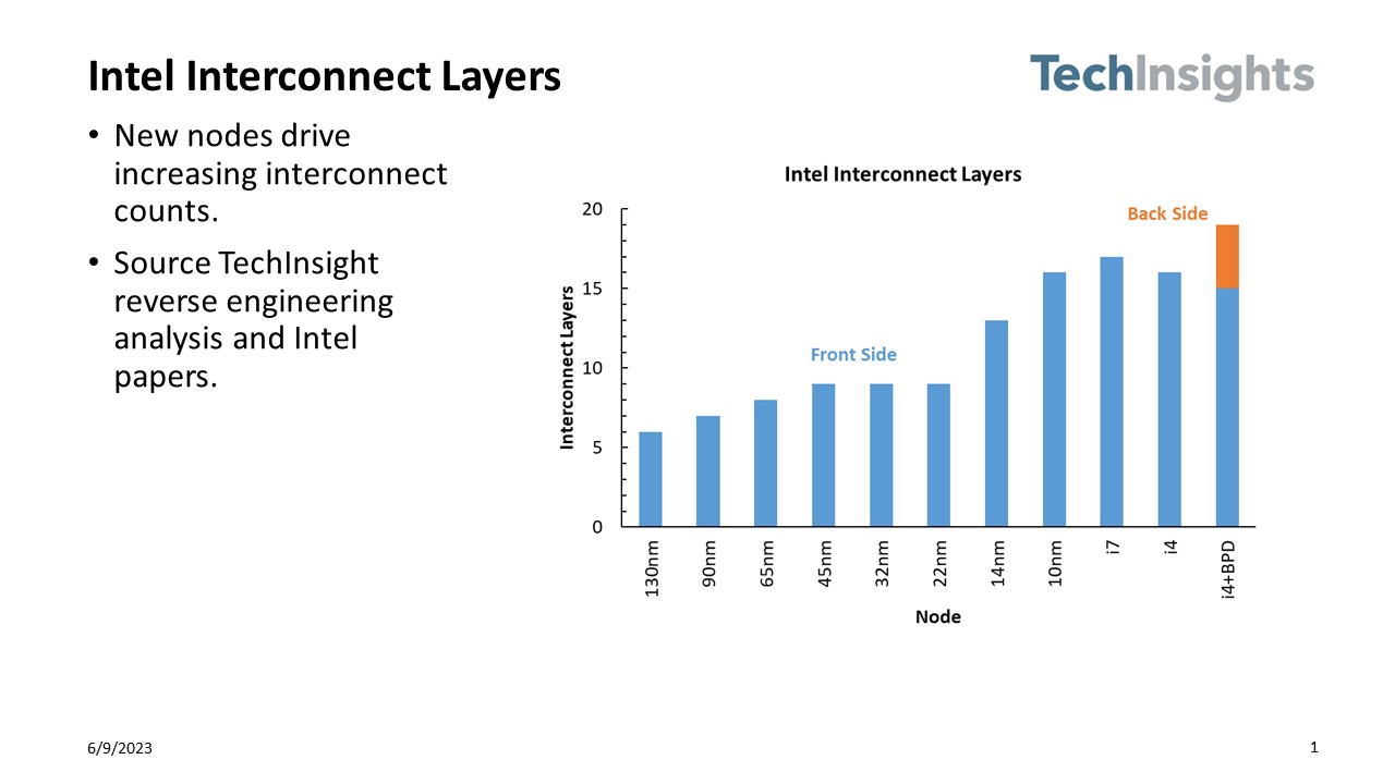
Please note that for recent nodes interconnect layers may vary by a few layers depending on the device.
Connections from the outside world to a device are made through the top interconnect layers and that means for power to get down to the devices, power must go through the entire interconnect stack via chain, see figure 3.
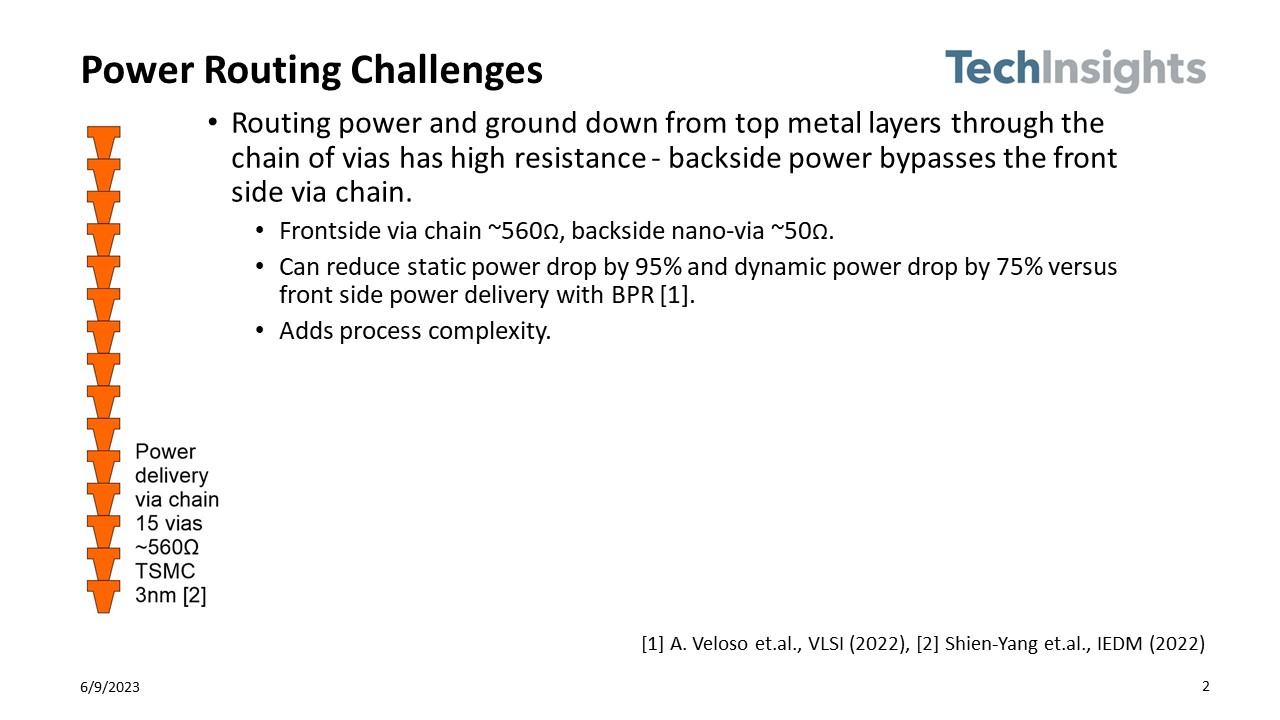
The example in figure 3 from TSMC’s 3nm technology shows a via chain resistance of 560 ohms versus imec reports of a backside nano-via of ~50 ohms. One of the key advantages of BS-PDN becomes clear.
Another advantage that Intel is talking about is cost. BS-PDN relaxes the requirements for metal zero lowering cost for the most expensive interconnect layer at the expense of relatively large pitch backside metal layers.
There are multiple approaches to BS-PDN. Imec is advocating for Buried Power Rails (BPR) as a connection point for BS-PDN. In figure 4. Intel shows a density advantage to Power Via versus BPR.
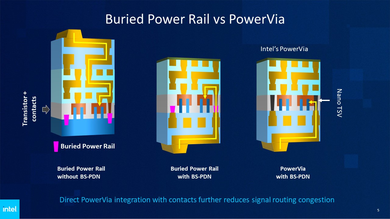
I have two comments about, first of all, my sense is the industry is reluctant to implement BPR because it requires metal buried in the wafer before transistor formation. In my discussions with imec they admit this reluctance but believe BPR will eventually be needed. I should also mention that imec believes BPR can also connect into the side of the device without going up to metal 0 and achieve the same or better density as Power Via, this is an area of contention between the technologies.
In order to minimize risk instead of running their first PowerVia tests on Intel’s 20A process that also introduces RibbonFET (Horizontal Nanosheets), Intel has run Power Via on the i4 FinFET process Intel is currently ramping up in production.
Figure 5. summarize the results seen with PowerVia on i4. Power Via has demonstrated improved Power, Performance, and Area (PPA).
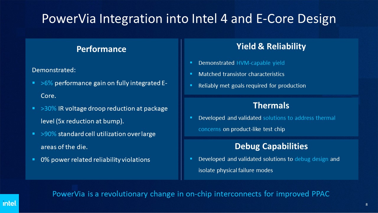
Figure 6. illustrates the area improvement and figure 7. Illustrates the power and performance advantages.
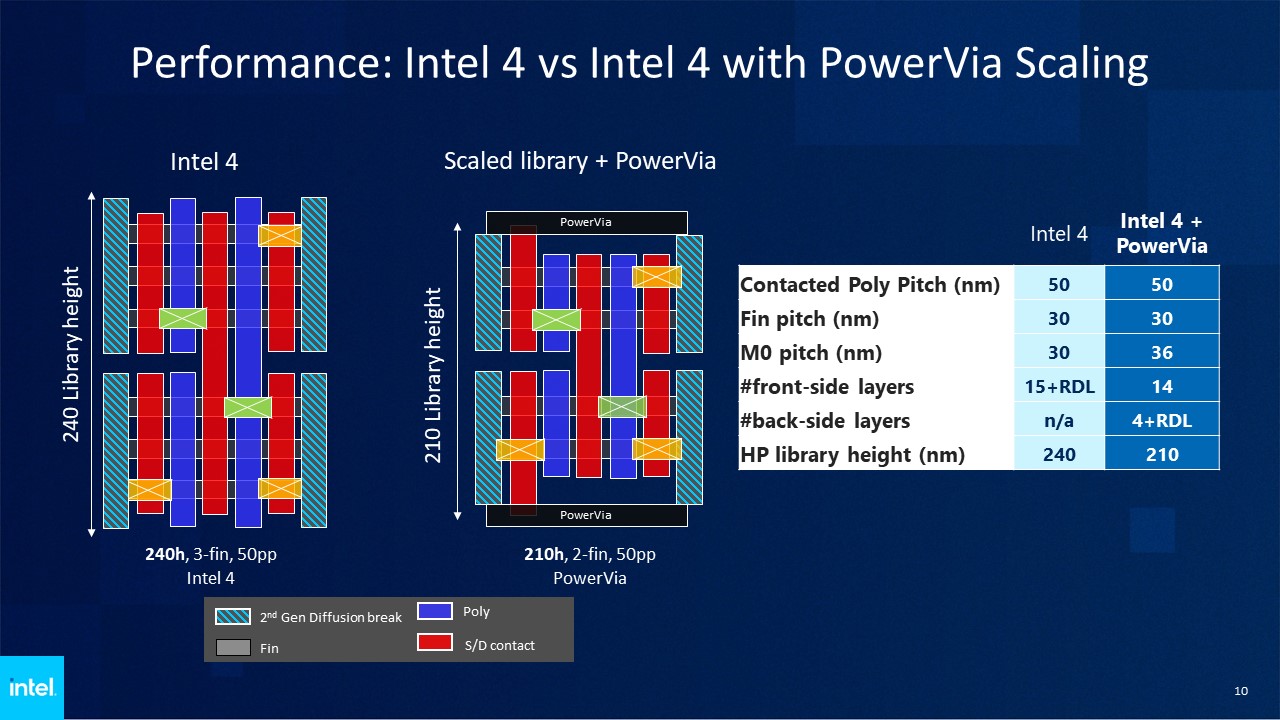
From figure 6 it can be seen that power via reduces the call height while also relaxing metal 0 from 30nm pitch to 36nm pitch. The relaxation in pitch likely results in a single patterned EIV layers versus multipatterned EUV.
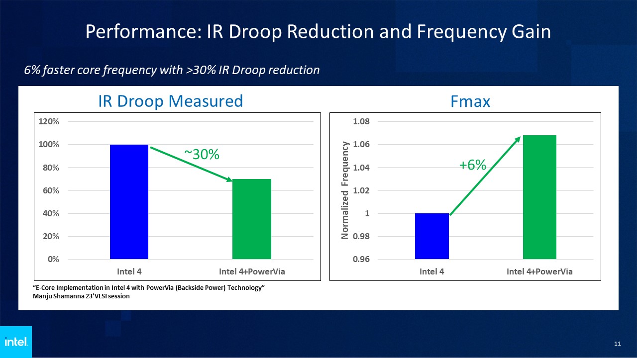
In figure 7 it can bee seen that IR Droop is reduced by 30% and Fmax is increased by 6%.
Finally, in figure 8 we can see that i4 = PowerVia yield is tracking i4 yield offset by 2 quarters.
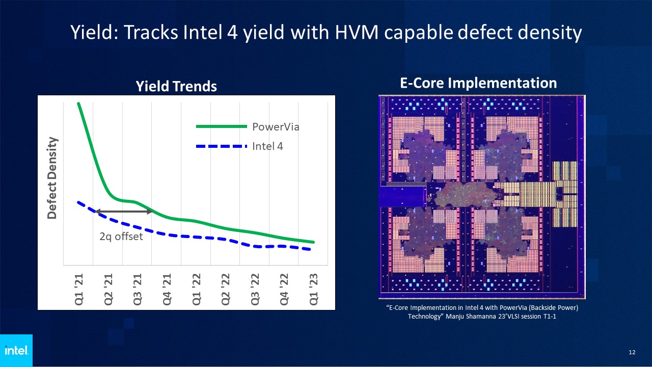
With PowerVia due to be introduced in 2024 on Intels 20A process in the first half and 18A in the second half, it appears that PowerVia should have minimal impact on yield.
It is interesting to note that Intel is planning to introduce PowerVia in 2024. Samsung and TSMC have both announced BS-PDN for their second generation 2nm nodes due in 2026, giving Intel a 2 year lead in this important technology. My belief is two fold, one Intel is continuing to make progress on the timely introduction of new technologies, and, two, Intel likely prioritized BS-PDN because they are more focused on pure performance that the foundries.
Here is the official Intel press release:
https://www.intel.com/content/www/us/en/newsroom/news/powervia-intel-achieves-chipmaking-breakthrough.html
Also Read:
IEDM 2022 – Ann Kelleher of Intel – Plenary Talk
Intel Foundry Services Forms Alliance to Enable National Security, Government Applications
Intel and TSMC do not Slow 3nm Expansion
How TSMC Contributed to the Death of 450mm and Upset Intel in the Process
Share this post via:


Comments
18 Replies to “VLSI Symposium – Intel PowerVia Technology”
You must register or log in to view/post comments.