You are currently viewing SemiWiki as a guest which gives you limited access to the site. To view blog comments and experience other SemiWiki features you must be a registered member. Registration is fast, simple, and absolutely free so please,
join our community today!
At the 2026 VLSI Symposium, Intel Foundry provided a detailed update on its process technology roadmap, highlighting the continued maturation of Intel 18A, the introduction of Intel 18A-P, and several advanced research initiatives that extend beyond current gate-all-around (GAA) transistor architectures. The presentation… Read More
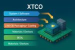
imec XTCO (Cross-Technology Co-Optimization) is the natural successor to DTCO and STCO in an era where no single layer of the stack can deliver scaling alone. Instead of optimizing devices, interconnect, packaging, architecture, and software in isolation, XTCO treats them as one tightly coupled system with a shared budget … Read More
The inaugural event for the 2025 TSMC Technology Symposium recently concluded in Santa Clara, California. This will be followed by events around the world over the next two months. We have summarized information from this event regarding process technology innovation and advanced packaging innovation. Overall, the A14 process… Read More
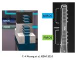
At IEDM 2023, Naoto Horiguchi presented on CFETs and Middle of Line integration. I had a chance to speak with Naoto about this work and this write up is based on his presentation at IEDM and our follow up discussion. I always enjoy talking to Naoto, he is one of the leaders in logic technology development, explains the technology in … Read More
I attended the recent International Electron Devices Meeting (IEDM) last week. Many of the sessions are too technical and too far away from high volume manufacture to make good topics for a blog post. As a Fellow from IBM said about 5nm at and earlier IEDM, “none of these ideas will impact 5nm. It takes ten years for a solution to from… Read More
Ann Kelleher is Intel’s Executive Vice President, General Manager, Technology Development, and she gave the first plenary talk to kick off the 2022 IEDM, “Celebrating 75 Years of the Transistor A Look at the Evolution of Moore’s Law Innovation”. I am generally not a fan of plenary talks because I think they are often too broad and… Read More
SEMICON West 2022 was held from July 12th to 14th at the Moscone Center in San Francisco.
On Monday the 11th before the show, Imec held a technology forum at the Marriott Marquee right around the corner from the Moscone center. In recent years the Imec forums have shifted away from the process technology I cover to more of a system and… Read More
At the recent VLSI Symposium on Technology and Circuits, Dr. Y.J. Mii, Senior Vice President of Research and Development at TSMC, gave a plenary talk entitled, “Semiconductor Innovations, from Device to System”. The presentation offered insights into TSMC’s future R&D initiatives, beyond the current roadmap. The associated… Read More
The VLSI Symposium on Technology and Circuits provides a deep dive on recent technical advances, as well as a view into the research efforts that will be transitioning to production in the near future. In a short course presentation at the Symposium, Marko Radosavljevic, from the Components Research group at Intel, provided … Read More
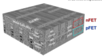
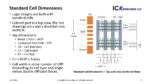
Standard Cell Scaling
Complex logic designs are built up from standard cells, in order to continue to scale logic we need to continually shrink the size of standard cells.
Figure 1 illustrates the dimensions of a standard cell.
Figure 1. Standard Cell Dimensions.
From figure 1 we can see that shrinking standard cell sizes requires… Read More