
At the 2021 Symposium on VLSI Technology and Circuits in June a short course was held on “Advanced Process and Devices Technology Toward 2nm-CMOS and Emerging Memory”. In this article I will review the first two presentations covering leading edge logic devices. The two presentations are complementary and provide and excellent overview of the likely evolution of logic technology.
CMOS Device Technology for the Next Decade, Jin Cai, TSMC
Gate length (Lg) scaling of planar MOSFETs is limited to approximately 25nm because the single surface gate has poor control of sub surface leakage.
Adding more gates such as in a FinFET where the channel is constrained between three gates yields the ability to scale Lg to approximately 2.5 times the thickness of the channel. FinFETs have evolved from Intel’s initial 22nm process with highly sloped fin walls to todays more vertical walls and TSMC’s high mobility channel FinFET implemented for their 5nm process.
Taller fins increase the effective channel width (Weff), Weff = 2Fh + Fth, where Fh is the fin height and Fth is the fin thickness. Increasing Weff increases drive current for heavily loaded circuits but excessively tall fins waste active power. Straight and thin fins are good for short channel effects but Fw is limited by reduced mobility and increase threshold voltage variability. Implementing a high mobility channel (authors note, SiGe for the pFET fin) in their 5nm technology gave TSMC an ~18% improvement in drive current.
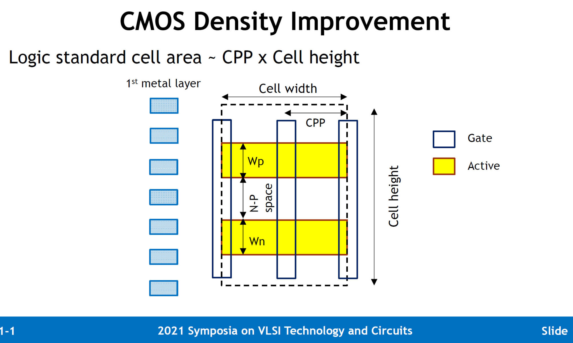
As devices scale down parasitic resistance and capacitance become a problem. Contacted Poly Pitch (CPP) determine standard cell widths (see figure 1) and is made up of Lg, Contact Width (Wc) and Spacer Thickness (Tsp), CPP = Lg + Wc + 2Tsp. Reducing Wc increases parasitic resistance unless process improvements are made to improve the contacts and reducing tsp increases parasitic capacitance unless slower dielectric constant spacers are used.

Figure 1. Standard Call Size.
As the height of a standard cell is reduced the number of fins per device has to be reduced (fin depopulation), see figure 2.

Figure 2. Fin Depopulation.
Fin depopulation reduced cell size increasing logic density and provide higher speed and lower power, but it does reduce drive current.
Transitioning from FinFETs to stacked Horizontal Nanosheets (HNS) enable increased flexibility by varying the sheet width (see figure 3.) and the ability to increase Weff by stacking more sheets.

Figure 3. Flexible Sheet Width.
Adding sheets adds to Weff, Wee = N*2(W+H), where N is the number of sheets, W is the sheet width and H is the sheet height (thickness). Ultimately the number of sheets is limited by the performance of the bottom sheet. The spacing between sheets reduces parasitic resistance and capacitance as it is reduced but must be big enough to get the gate metals and dielectric into the gap. There is a bottom parasitic mesa device under and HNS stack that can be control by implants or a dielectric layer.
In FinFET nFET electron mobility is higher than pFET hole mobility. In HNS the mobility is even more unbalanced with higher electron mobility and lower hole mobility. Hole mobility can be improved by cladding the channel with SiGe or using a Strain Relaxed Buffer but both techniques add process complexity.
Imec has introduced a concept called a Forksheet (FS) where a dielectric layer is put between the nFET and pFET reducing the n-p spacing resulting in a more compact standard cell, see figure 4.

Figure 4. Forksheet.
Beyond a HNS with FS, there is the Complementary FET (CFET) that stacks the nFET and pFET eliminating the need for horizontal n-p spacing.

Figure 5. CFET.
CFET options include monolithic integration where both nFET and pFET devices are fabricated on the same wafer and sequential integration where the nFET and pFET are fabricated on separate wafers that are then bonded together, both options have multiple challenges that are still being worked on.
Beyond CFET the presenter touched on 3D integration with transistor integrated into the Back End Of Line (BEOL) interconnect. These options require low temperature transistors with polysilicon channels or oxide semiconductors presenting a variety of performance and integration challenges.
In the Front End Of Line (FEOL) options beyond CFETs are being explored such as high mobility materials, Tunnel FETs (TFET), Negative Capacitance FETs (NCFET), Cryogenic CMOS and low dimensional materials.
Low dimensional materials make take the form of nanotubes or 2D Materials, these materials offer even shorter Lg and lower power than HNS but are still in the early research phase. Low dimensional materials also fit into the HNS/CFET approach with the option to stack up many layers.
Nanosheet Device Architecture to Enable CMOS Scaling in 3nm and beyond: Nanosheet, Forksheet and CFET, Naoto Horiguchi, Imec.
This section of the course expanded on the HNS/FS/CFET options discussed in the previous section.
As FinFETs are being scaled to the limits, fins are getting taller, thinner and closer. Fin depopulation is reducing drive current and increasing variability, see figure 6.

Figure 6. FinFET scaling.
The state-of-the-art today is a 6-track cell with 2 fins per device. Moving to single fins and narrower n-p spacing will require new device architectures to drive performance, see figure 7.

Figure 7. 6-Track Cell
To continue CMOS scaling we need to transition from FinFET sot HNS to HNS with FS and then CFETs, see figure 8.

Figure 8. Nanosheet Architectures for CMOS Scaling.
Transitioning from FinFETs to HNS offer several advantages, great Weff, improved short channel effect which means shorter Lg and better design flexibility due to the ability to vary the sheet width, see figure 9.

Figure 9. FinFET to HNS.
The presenter went on to go into detail on HNS processing and some of the challenges and possible solutions. A HNS process is very similar to FinFET processing except for four main modules, see figure 10.

Figure 10. HNS Process Flow.
Although a HNS flow is similar to a FinFET flow the key modules that are different are difficult. The release etch and achieving multiple threshold voltages is particularly difficult. There was a lot of good information on the specifics of the process modules changes required for HNS that is beyond the scope of a review article like this. One thing that wasn’t explicitly discussed is that in order to scale a HNS process to a 5-track cell Buried Power Rails (BPR) are required and that is another difficult process module that is still being developed.
As seen in the previous presentation further scaling of HNS can be achieved by FS. Figure 11 presents a more detailed view of how a dielectric wall shrinks a HNS cell.

Figure 11. Horizontal Nanosheet/Forksheet Structure Comparison.
The FS process requires the insertion of a dielectric wall to decrease the n-p spacing, figure 12 illustrates the process flow.

Figure 12. Forksheet Process Flow.
Beyond FS, CFET offers zero horizontal n-p spacing by stacking devices. Figure 13. Illustrates the CFET concept.

Figure 13. CFET Concept.
CFETs are particularly interesting for SRAM scaling. SRAM scaling has slowed and is not keeping up with logic scaling. CFET offer the potential to return SRAM scaling to the historical trend, see figure 14.

Figure 14. SRAM Scaling with CFET.
As previously mentioned there are two approaches to CFET fabrication, monolithic and sequential. Figure 15 contrasts the two approaches with pluses and minuses for each.

Figure 15. CFET Fabrication Options.
Conclusion
This review presented some of the key points of the two presentations leading edge logic devices. This is just an overview of the excellent and more detailed information presented in the course. The course also covered interconnect, contacts, and metrology for logic, and emerging memory, 3D memory and DRAM. I highly recommend the short courses.
Also Read:
Is IBM’s 2nm Announcement Actually a 2nm Node?
Ireland – A Model for the US on Technology
How to Spend $100 Billion Dollars in Three Years
Share this post via:


Comments
3 Replies to “VLSI Symposium – TSMC and Imec on Advanced Process and Devices Technology Toward 2nm”
You must register or log in to view/post comments.