TSMC recently announced plans to spend $100 billion dollars over three years on capital. For 2021 they announced $30B in total capital with 80% on advanced nodes (7nm and smaller), 10% on packaging and masks and 10% on “specialty”.
If we take a guess at the capital for each year, we can project something like $30B for 2021 (announced), $33.5B for 2022 and $36.5B for 2023. $30B + $33.5B + $36.5B = $100B. The exact breakout by year for 2022 and 2023 may be different than this but overall, the numbers work. If we further assume that the 80% spending on advanced node ratio will be maintained over the three years, we get: $24B for 2021, $26.8B for 2022 and $29.2B for 2023 ($80B total).
What kind of advanced capabilities can you buy for $80B over 3 years?
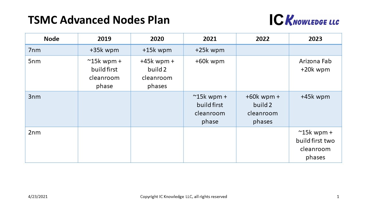
Figure 1 illustrates our view of TSMC’s advanced node plans.

Figure 1. TSMC Advanced Node Plans.
To begin 2021, TSMC had record 7nm revenue in Q1 and we believe they needed to add 25K wafer per month (wpm) of capacity to do that, whether that spending was in 2021 or late 2020 is subject to debate. 5nm was in production beginning in the second half of 2020 and we believe a farther ramp up of 60k wpm will take place in 2021 reaching 120k wpm by year end. Also, in late 2021 will be 3nm risk starts requiring the completion of one cleanroom phase and an estimated 15k wpm of 3nm capacity.
2022 will see the ramp up of 3nm with an additional 60K wpm of capacity.
2023 Will see the build out of 5nm capacity at the Arizona fab, and an additional 45k wpm of 3nm capacity. Finally, we expect 2nm risk starts in 2023 requiring a cleanroom build out and 15k wpm. Where 5nm and 3nm are being produced in 3 cleanroom phases each, TSMC has announced that 2nm will be built in four cleanroom phases and we have planned on two phase in 2023.
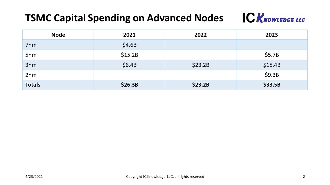
Figure 2 illustrates our view of TSMC’s capital spending by node for 7nm, 5nm, 3nm and 2nm.

Figure 2. TSMC Capital Spending on Advanced Nodes.
In 2021 we have $4.6B for 7nm capacity, $15.2B for additional 5nm capacity and $6.4B for the initial 3nm cleanroom and risk starts capability. The total $26.3B is more than the calculated $24B so some of the 7nm capacity may be in 2020 or some of the 3nm spending may be in 2022.
In 2022 we have $23.2B for additional 3nm capacity, this is less than the $26.8B expected for 2022. Because 2023 is expected to have spending in Arizona, more 3nm capacity and the initial 2nm build out it is possible 2022 may see less capital spending than we initially assumed and 2023 more capital spending.
For 2023 we have the first 5nm phase built out in Arizona for $5.7B, additional 3nm capacity for $15.4B and the initial build out of 2nm for $9.3B. The total for 2023 is $33.5B, more than the estimated $29.2B.
If we add up our forecast over three years, we get $79.8B versus the $80B estimate assuming 80% of the announced $100B is spent on advanced nodes. We should also keep in mind that the $100B is a three-year estimate subject to changing market conditions.
In this scenario, in 2023 TSMC will have 140k wpm of 5nm production capacity, 120k wpm of 3nm production capacity and 15k wpm of 2nm risk start capacity.
Also Read:
SPIE 2021 – Applied Materials – DRAM Scaling
Kioxia and Western Digital and the current Kioxia IPO/Sale rumors
Share this post via:


Comments
12 Replies to “How to Spend $100 Billion Dollars in Three Years”
You must register or log in to view/post comments.