
There are a lot of articles out right now discussing a possible IPO for Kioxia or sale of the company with Western Digital (WD) and Micron Technology (MT) mentioned as possible acquirers. Kioxia and WD have a partnership for Flash Memory and on March 18th WD gave a presentation on the state of their partnership and what they see as their competitive advantage. With all the recent discussion I though it would be useful to look at Kioxia, how they got to where they are, how the partnership with WD works and what their competitive position is.
Early Flash History
At the 1984 International Electron Devices Meeting, Masuoka, et.al., of Toshiba disclosed the idea of an electrically programable – non-volatile memory that could be rapidly erased in blocks (Flash is for flash erase). The architecture only required a single transistor per memory cell rather than 2 transistors per cell the way standard EEPROM did. This was the beginning of Flash memory technology.
Early Flash memory was weighted towards NOR Flash that was used primarily for code storage. In 1986 Intel invented ETOX Flash and even as late as 2000 Intel was the leading producer of Flash memory with NOR Flash although Intel eventually exited the Flash business before returning to make 3D NAND Flash with Micron.
Around 2005 NAND Flash passed NOR Flash in revenue finding applications in digital cameras, mp3 players, USB memory sticks and other data storage applications. By 2010 NAND Flash represented over 80% of Flash memory revenue and that percentage has continued to grow with increasing use for disk drives and in cell phones.
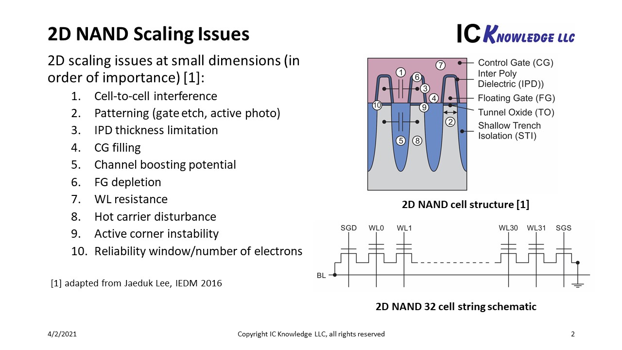
Up until the mid 2010’s 2D NAND Flash production grew rapidly and led the semiconductor industry with the smallest linewidths, for example 2D NAND was the first application to make use of Self Aligned Quadruple Pattering (SAQP). Eventually 2D NAND Flash cells became so small that a variety of issues drove the need for a new solution, see figure 1.

Figure 1. 2D NAND Scaling Issues.
During this time Toshiba became a leading producer of 2D NAND.
3D NAND
In 2007 at the VLSI Technology Symposium, Toshiba disclosed Bit Cost Scalable Technology (BiCS) for 3D NAND. The BiCS process that was disclosed created a memory stack by depositing alternating layers of silicon oxide and polysilicon and then etching down through the stack to form multiple memory cells in a vertical array. This was a gate first technology and is illustrated in figure 2.

Figure 2. Toshiba BiCS Process.
In 2009 at the VLSI Technology Symposium Samsung disclosed their Vertical Cell Array using TCAT (Terabit Cell Array Transistor) Technology for 3D NAND. TCAT memory array fabrication begins with alternating layers of silicon oxide and silicon nitride and then etching down through the stack to form multiple memory cells in a vertical array. The nitride is eventually removed and replaced with metal layers for the gate and word line (replacement gate).
The TCAT process is illustrated in figure 3.

Figure 3. Samsung TCAT Process.
The basic idea of 3D NAND is to turn the 2D NAND string on end into the vertical direction, see figure 4.

Figure 4. 3D NAND Structure.
The key differences between BiCS and TCAT are:
- A BiCS memory array stack is oxide and poly layers and TCAT memory stack is oxide and nitride layers.
- In a BICS memory array the poly is left in place and becomes the gates and word lines (gate first). In a TCAT memory array the nitride is removed and replaced with gate metals and tungsten for the gate and word line (replacement gate).
As 3D NAND was being developed there were rumors in the industry that Toshiba could not get BiCS to yield and in fact in around 2014/2015 when the first commercial parts began to filter out, construction analysis done by our strategic partner Tech Insights showed that Toshiba had essentially copied Samsung’s TCAT process. Interestingly Toshiba continued to refer to their process as BiCS even though BiCS and TCAT are fundamentally different processes. I suppose what Toshiba was doing was still “punch and plug” as discussed in the original BiCS paper but in my opinion the process Toshiba took to production is clearly not BiCS.
Kioxia/Western Digital
Due to large losses in their Westinghouse nuclear power division, Toshiba spun out their NAND Flash business into Toshiba Memory and eventually Toshiba Memory was further spun out to an investment consortium led by Bain Capital becoming Kioxia. The approximate ownership shares in Kioxia are Bain at 50%, Toshiba at 40% and Hoya at 10%.
Back when Kioxia was a Toshiba division, Toshiba and SanDisk formed a partnership for Flash memory. Eventually WD bought SanDisk, Toshiba Memory became Kioxia, and Kioxia and WD became partners in Flash memory in a joint venture known as Flash Ventures (FV). FV is owned ~50/50 by WD/Kioxia and the wafer output is split ~50/50.
As I understand the joint venture, Kioxia builds the fabs, Kioxia and WD share the capital expense of equipping the fabs and they share the fabs output with both companies selling Flash memory. In a recent note, Well Fargo noted that the joint venture currently extends to 2034+ presenting a complication to any attempt to acquire Kioxia. The Japanese government also played a role in Kioxia’s formation vetoing too much foreign ownership.
Western Digital Presentation
On March 18, 2021, Dr. Siva Sivaram of WD gave a Flash Technology Overview of the Kioxia/WD partnership. I thought it would be interesting to examine some of the statements that were made in the presentation.
WD and Kioxia have invested a combined $18 billion dollars in Flash R&D in the last ten years, they believe this is the largest investment specific to Flash in the industry. I do not have any data to compare this to.
WD and Kioxia claim >34% of worldwide NAND bits shipped versus 33% for Samsung making the combined entity the world’s largest producer of NAND Flash. I reached out to Bill McClean at IC Insight’s and he provided the NAND revenue breakout shown in figure 5, Samsung has slightly more revenue share than Kioxia/WD. It is entirely possible Kioxia/WD ship slightly more bits and Samsung has slightly higher revenue, overall, I would say that Kioxia/WD is neck and neck with Samsung.

Figure 5. Worldwide NAND Revenue by Company. Figure provided by IC Insight’s.
And interesting note on this, Samsung has revenue of $18.2 billion dollars growing at 21%, Kioxia/WD have combined revenue of $17.6 billion dollars growing at 23% and SK Hynix/Intel has revenue of $11.8 billion dollars growing at 45% (SK Hynix is acquiring the Intel Flash business).
The Yokkaichi fab complex has seen $40 billion dollars in total investment and has over 550 thousand wafers per month capacity (kwpm) making it the second largest capacity fab complex in the world. The reported >550kwpm capacity was somewhat surprising to me, Kioxia has been shedding 2D NAND capacity and a few years ago that number would have made sense to me, but I thought their capacity was closer to 500kwpm in Yokkaichi (Kioxia has another Fab in Kitakami City, Iwate prefecture).
Figure 6 illustrates our estimates for 2D NAND and 3D NAND capacity by company and wafers run.

Figure 6. 2D and 3D NAND Wafer Capacity and Total NAND Wafers Run by Company for 2020.
From figure 6, Kioxia has the highest total NAND capacity but they appear to have more 2D NAND capacity than their competitors and their Fabs are the least utilized. We believe they are shedding 2D NAND capacity currently while also building new 3D NAND capacity. I should note, that getting good visibility on actual 2D versus 3D NAND capacity for Samsung and Kioxia is challenging, and these are best estimate numbers.
During the presentation, several times WD claimed that Kioxia/WD have the best 3D memory cell in the business, I am not sure how they determine this. The physical analysis I have seen from Tech Insights shows identical material sets for the memory cell from Kioxia and Samsung with the only difference being film thicknesses, see figure 7.

Figure 7. Kioxia Versus Samsung Memory Cell.
The thicknesses differences could result in different performance or something about deposition and clean conditions could possibly give Kioxia an advantage in their cell, but it is not clear to me what it actually is or what they are measuring to claim leadership.
WD also claimed multibit leadership and they may have been first for 3 bits per cell – triple level cell (TLC) flash but I believe Intel-Micron was first to 4 bits per cell – quadruple level cell (QLC).
WD claimed that they scale laterally more than the other players and therefore have more bits with fewer layers saving cost. There are multiple elements that go into bit density:
- Within the memory array area, bits scale up with number of layers.
- Horizontal scaling can increase number of bits per unit area of memory array and could give an advantage in bits per unit area per layer.
- Whether CMOS is fabricated next to the memory array or partially under the memory array is a determining factor in what percentage of a die is memory array.
Figure 8. presents an analysis of several generations of 3D Flash parts for layers, bits per millimeter squared, and bit per millimeter squared per layer.

Figure 8. Memory Density.
For each company, Kioxia, Micron (charge trap only), Samsung and SKH there are three columns. The first column is number of layers for the generation, the second column is the bit capacity of the die divided by the die area, the third column is the second column divided by the first column to get bits per millimeter squared per layer.
Black numbers are measured on production parts or conference disclosed numbers, red is our estimates based on layers scaling and forecast for CMOS on the side or under the array. Bold numbers are the leaders for each generation.
Another side note, in their ISSCC 2021 presentation, Kioxia presents 3.88Gb/mm2 for 64L versus our measured density of 3.40Gb/mm2. The ISSCC presentation is for a 512Gb part and the part Tech Insights measured is 256Gb. Similarly, at 96L the ISSCC value is 5.95Gb/mm2 for a 512Gb part and the part Tech Insights measured is once again a 256Gb part. Interestingly the presentation lists a 128L part with 7.8 Gb/mm2 when Kioxia went into production with a 112L part, and they also list 10.45Gb/mm2 for a 170L+ part when their production announcement is 162L. So, there is some disconnect between their presentation and production practices.
Our analysis has SK Hynix leading for bit density and bits per layer at 48 layers, SK Hynix leading for bit density at 64/72 layers but Samsung and Kioxia tied for the bits per layer lead. At 92/96 layers SK Hynix once again leads for both categories. At 112/128 layers we expect Micron to lead for bit density but Kioxia to have the best bits per layers and finally at 160/162/176 layer we expect Micron to lead in both categories. Of course, the Micron values at 112/128 layers and 162/176 are only as good as our forecast and we should note we have not seen any Micron charge trap part analysis yet, so these forecasts are scaled from Micron’s Floating Gate work with Intel. The bottom line is Kioxia appears to be competitive but not be a consistent leader.
The bottom line is who delivers the lowest bit cost, IC Knowledge is the world leader in cost modeling of semiconductor and MEMS. Using our Strategic Cost and Price Model – 2021 – revision 00a we have evaluated wafer cost and bit cost for three generations of 3D NAND by company. Figure 9 presents relative wafer cost, density, and bit cost.

Figure 9. Cost Leadership.
In figure 9 we did not analyze beyond the 112L/128L generation because we are currently updating the model to the latest announced layer counts.
Samsung is the wafer cost leader at all layer counts, this is due to Samsung being the last company to string stack and the last company to put CMOS partially under the memory array. This results in lower wafer cost but eventually the density is not competitive, and Samsung loses out on cost per bit.
The bit cost leadership changes from Samsung at 64L/72L, to SK Hynix at 92L/96L, to Micron at 112L/128L. As mentioned on the figure Micron is the least certain part of the analysis and is subject to change once we see actual measured parts.
In terms of Kioxia, we do not see them the leader in any of the three factors at any layer count analyzed. The Kioxia bit cost is competitive for their 64L process and 112L processes but not at 96L.
In summary we believe Kioxia is a competitive 3D NAND player and particularly strong in bits per millimeter squared per layer, but we would question whether they have the level of leadership represented in the WD presentation.
IPO or Acquisition
This is outside of my specific expertise; it does seem to me that an acquisition by Micron would be difficult with the FV JV in place until 2034+. We estimate WD/SanDisk has invested over $18 billion dollars in equipment located in the Kioxia fabs, how that would be handled in an acquisition and the supply commitments, strikes us as problematic. WD would be the most obvious acquirer, WD did try to acquire Kioxia when they were spun out but lost out to the consortium led by Bain. In a Wells Fargo analysis note they have raised concerns about WD ability to handle an acquisition of the size of Kioxia with a $30 billion price tag mentioned. There may also be issues with the Japanese government blocking the sale of Kioxia to a non-Japanese entity. It seems to me that the most likely outcome is an IPO when the time is right.
Also Read:
ISS 2021 – Scotten W. Jones – Logic Leadership in the PPAC era
Share this post via:


Comments
8 Replies to “Kioxia and Western Digital and the current Kioxia IPO/Sale rumors”
You must register or log in to view/post comments.