On Monday morning at IEDM, Sri Samavedam of Imec opened the technical program with a plenary talk entitled “Future Logic Scaling: Towards Atomic Channels and Deconstructed Chips”. I am not generally a fan of plenary talks, I think the presenters often try to cover too much in their talks and end up not providing enough detail to be useful, but there was a lot of good content in this talk.
I asked Imec for the slides to include some of them in this article, but they declined to provide them although they did send me the paper. I find it strange that they will not provide the slides, the video presentation of the slides is on the IEDM web site for registered attendees to view and anyone with a screen capture utility can easily capture any or all the slides. I will make use of a couple of the figures from the paper to try to make up for the lack of the slides.
The first approximately seven minutes of the talk were justifying the need for continued development of leading-edge technology and some historical perspective, I am going to omit this part as I believe the average Semiwiki reader and IEDM participant understand this already.
EUV Patterning
The talk then jumped into an EUV patterning roadmap. The presenter stated he thought High-NA EUV will be available for path finding around 2023 and will need two to three years to be ready for production. This would result in High-NA EUV entering production in the 2025/2026 timeframe, significantly later than I would have expected.
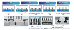
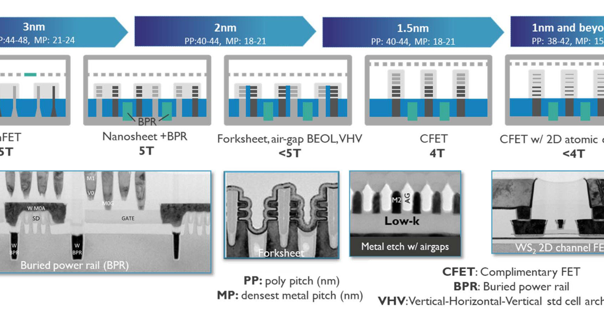
The Imec roadmap is for 3nm logic nodes to have 44-48nm Contacted Poly Pitch (CPP) and 21-24nm Minimum Metal Pitches (MMP), the 2nm logic node to be 40-44nm CPP and 18-21nm MMP and the 1.5nm logic node to be 40-44nm CPP, and 18-21nm MMP. I expect TSMC to be make risk starts with a 3nm node in late 2021 and production in 2022 and the CPP and MMP to be in the range of the numbers Imec proposes. I expect TSMC’s 2nm node to make risk starts in 2023 and production in 2024 and once again to have CPP and MMP values in the range that Imec presented. For 1.5nm Imec does not show any reduction in CPP and MMP ranges presumably reflecting a change to stacked transistors (more on this later) as a technique to drive density.
The Imec roadmap shows the current 0.33NA EUV systems being used for 3nm and 2nm and High-NA (0.55NA) being introduced at the 1.5nm node, this is once again later than I expected. I have for some time expected High-NA EUV to miss the 3nm node (although others have discussed high-NA for 3nm), but I thought the systems would be available for 2nm. If High-NA EUV systems are not available until 1.5nm it would be strictly as a cost reduction technique since 1.5nm has the same pitches as 2nm, and 2nm would already have been in production. Several years ago, I gave a presentation to ASML and raised the idea that by the time High-NA EUV was available transistor stacking (CFETs) might make it irrelevant. While it is likely that High-NA EUV can provide a cost reduction versus multi-patterning with EUV, if this timeline is correct it will not be a technology enabler.
I reached out to ASML for a comment on this and got the following reply:
“We are aligning with customers on roadmap timing of High NA insertion in volume production, currently estimated to be in the 2025-2026 timeframe. We will work with them to ramp to HVM as quickly as possible. Looking back at prior transitions, like ArFi, usually it takes a couple of years to ramp to HVM after first tool shipments. So a 2025-2026 HVM timing would help our customers reduce use of EUV multiple patterning and provide benefits in cost, process complexity, and cycle time.”
Logic Scaling
One of my favorite slides in the presentation is the Logic Scaling Roadmap slide and thankfully it is a figure in the paper (see figure 1.)

Figure 1. Logic Scaling Roadmap
For the 3nm node Imec shows a 5-track height cell based on a FinFET, this is the approach that I believe TSMC is taking. Samsung on the other hand has announced they will use Gate All Around at 3nm (a Horizontal Nano Sheet, HNS) and I believe this will be a 6-track height cell because to get to 5-tracks with HNS requires Buried Power Rails (BPR) and BPR is not ready for production yet (Samsung 3nm will be significantly less dense than TSMC 3nm based on the companies announced density improvements).
At 2nm, 5-track HNS utilizing BPR is an option or even HNS with a Fork Sheet (FS) to enable a less than 5-track cell (Authors note: ~4.33-tracks may be possible by combining HNS, BPR and FS).
Moving forward to 1.5nm CFETs with nFET and pFET stacking and 4-track cells can provide a shrink while maintaining the same pitches as 2nm. Imec is doing a lot of research on CFETs, Intel presented an interesting paper on CFETs at the conference that utilized three pFETs and two nFETs in a stack to match the performance of the two device types, and Synopsys also presented on CFETs in a paper that I was a coauthor on.
For 1nm and beyond Imec is working on 2D atomic channels and less than 4-track cells. There is also work that I am aware of to further extend CFETs by stacking more layers. 2D atomic channels would be stacked up like nanosheets but due to the extremely thin layers potentially provide higher frequency performance at the same power.
The presentation went on to further discuss BPR. BPR can lower the power delivery resistance improving power efficiency and provide an area reduction by creating tall metal lines in the substrate to replace wide metal lines in the interconnect layers. BPR can also enable power delivery networks on the back of a wafer that connect to BPR by using through silicon vias (TSV) although this requires very small “nano” TSVs. Utilizing the backside of the wafer for power delivery would also enable Metal Insulator Metal (MIM) Capacitors and Electrostatic Discharge (ESD) protection diodes to be integrated on the backside.
Beyond 2D atomic channel transistors, Imec is investigating various option including Qubits for quantum computing.
BEOL Roadmap
Looking at the Back End of Line (BEOL) Imec believes copper dual damascene can scale to a 21nm pitch but via resistance will be a problem. To address via resistance a hybrid scheme is needed where the vias are fabricated with an alternative material such as ruthenium, molybdenum, or tungsten. 3nm node processes are defined in the Imec roadmap as having pitches of 21-24nm so standard dual damascene copper is probably OK for the 3nm node. In the Imec roadmap the 2nm node has 18-21nm metal pitches so hybrid metallization will likely be required for the most critical layers.
Beyond 21nm pitch, subtractive metal patterning becomes attractive to enable high aspect ratio metal lines with partial or full air gaps to address line to line capacitance. Because copper is so hard to dry etch, subtractive metallization will require new metals such as Ruthenium or Molybdenum. The combination of Semi Damascene (with subtractive patterning) and air gaps results in a significant reduction in the resistance-capacitance (RC) of the interconnect. Imec has demonstrated 32nm pitch and is currently working on 18nm pitch. The initial 18nm results show better RC performance but still need work on self-aligned vias and air gap fabrication. Semi Damascene is a candidate for the 1.5nm node.
Beyond the 1.5nm node Imec is investigating alternative materials. The figure of merit for materials at very small dimensions is the bulk resistivity multiplied by the electron mean free path, this is because at small dimensions materials with long electron mean free paths, see a significant increase in resistivity. Imec has identified several promising alloys in simulations and needs to work through the integration challenges and demonstrate the materials are viable on actual devices.
SRAM Scaling
Continued logic scaling has been enabled by design technology co-optimization enabling track height reductions but this does not carry over to SRAM cells. Where SRAM cell sizes once scaled at 50% per node that scaling has slowed. A move to HNS will provide some gate length scaling but limitations on sheet width will limit scaling. FS can provide a scaling boost and CFETs can offer additional reductions.
There are also opportunities to utilize sequential 3D integration schemes and fabricate logic over SRAM arrays on pre-processed wafers, but this technique would require low temperature processing of the logic without compromising performance.
Deconstructed Chips
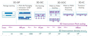
Increasingly capable 3D integration schemes offer the ability to deconstruct chips into multiple chips with each chip optimized for its function. Breaking up a complex system on chip (SOC) design into chiplets would allow optimized chiplets, for example one chiplet could be a processor core, other chiplets could be SRAM cache lower-level cache, MRAM or DRAM for higher levels cache or main memory all integrated with very high band width. Specialty devices fabricated with compound semiconductors could also be integrated. In order to realize the full potential of deconstructed 3D integration improvements in wafer to wafer bonding, micro bumps and power dissipation challenges need to be overcome.
Figure 2. illustrates Imec’s view of the 3D integration landscape.

Figure 2. 3D Integration Landscape.
Conclusion
The technologies discussed here offer ten to fifteen more years of logic scaling. EUV patterning with the 0.33NA to High-NA (0.55NA) transition, HNS, FS, BPR, PDN, CFETs and 2D atomic channels, new SRAM scaling techniques and 3D Integration are all promising candidates for future logic technologies.
Also Read:
No Intel and Samsung are not passing TSMC
Leading Edge Foundry Wafer Prices
VLSI Symposium 2020 – Imec Monolithic CFET
Share this post via:


Comments
There are no comments yet.
You must register or log in to view/post comments.