You are currently viewing SemiWiki as a guest which gives you limited access to the site. To view blog comments and experience other SemiWiki features you must be a registered member. Registration is fast, simple, and absolutely free so please,
join our community today!
In the modern world, the semiconductor industry stands at the heart of technological innovation. From smartphones and laptops to advanced medical devices and artificial intelligence systems, nearly every piece of contemporary electronics depends on increasingly sophisticated microchips. Among the leading companies … Read More
By Zameer Mohammed
This article claims to provide clear key insights of Min Pulse Width (MPW) timing signoff check, proactive closure strategies for faster time-to-market, and effective methods to prevent silicon failures.
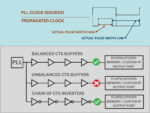
Min Pulse Width (MPW) check for timing signoff has become an important design constraint at the sub-5nm… Read More
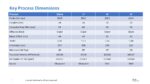
At the VLSI Technology Symposium this week Intel released details on their i3 process. Over the last four nodes Intel has had an interesting process progression. In 2019, 10nm finally entered production with both high performance and high-density standard cells. 10nm went through several iterations eventually resulting in… Read More
Throughout the debate on fab incentives and the Chips Act I keep seeing comments like; TSMC makes >90% of all advanced silicon, or sometimes Taiwan make >90% of all advanced silicon. This kind of ill-defined and grossly inaccurate statement drives me crazy. I just saw someone make that same claim in the SemiWiki forums and… Read More
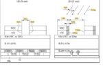
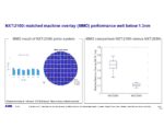
The majority of EUV production is on 5nm and 3nm node, implemented by late 2022. Metal oxide resists have not been brought into volume production yet [1,2], meaning that only organic chemically amplified resists (CARs) have been used instead until now. These resists have a typical absorption coefficient of 5/um [3,4], which means
…
Read More
- Reports suggest Intel will get 6 of 10 ASML High NA tools in 2024
- Would give Intel a huge head start over TSMC & Samsung
- A big gamble but a potentially huge pay off
- Does this mean $4B in High NA tool sales for ASML in 2024?
News suggests Intel will get 6 of first 10 High NA tools made by ASML in 2024
An industry news source, Trendforce, reports… Read More
As integration levels increase, clock frequencies rise, and feature sizes shrink it is not surprising that all or most aspects of semiconductor design become more complex and demand more from design technologies. One example where the traditional approach is breaking down is in optimizing power distribution networks (PDNs)… Read More
At SEMICON West I had a chance to catch up with Mike Lercel of ASML. In this article I am going to combine ASML presentation material from the SPIE Advanced Lithography Conference, Mike’s SEMICON presentation, my discussions with Mike at SEMICON and a few items from ASML’s recent earnings call.
DUV
ASML continues to improve DUV systems.… Read More
On May 22nd Applied Materials announced a new development center, Equipment and Process Innovation and Commercialization Center (EPIC).
Applied Materials already operates the Maydan Technology Center (MTC), a billion-dollar development facility with over 120 advanced process tools and 80 metrology and inspection tools… Read More
I don’t know the story behind the name Alchip. I’ve been asking this question ever since its founding in 2003 and still haven’t found the answer. Wikipedia sometimes provides insights and stories behind names of companies, products and services but I couldn’t find any regarding the name Alchip. One thing is for sure. After its consistent… Read More