I was invited to give a plenary address at the SISPAD conference in September 2021. For anyone not familiar with SISPAD it is a premiere TCAD conference. This year for the first time SISPAD wanted to address cost and my talk was “Cost Simulations to Enable PPAC Aware Technology Development”.
For many years the standard in technology development has been Power, Performance and Area (PPA), for example: on TSMC 2020-Q4 earnings call, N3 will have 30% lower power at the same performance (Power), 15% greater performance at the same power (Performance) and 70% greater density (Area).
More recently increasing wafer costs are driving the need to add cost as PPAC, Power, Performance, Area and Cost. Companies such as TSMC at IEDM 2019 [1], Imec at their technology forum in 2020 [2] and Applied Materials at SEMICON West in 2020 [3], and many others are all taking about PPAC.
The current practice when developing a new technology is to define initial PPA targets, identify designs for PPA evaluation, select a transistor architecture, develop an initial process flow, simulate transistor performance, and extract a SPICE model, select a standard cell architecture, and generate a cell library. The cell library and process flow are then fed into a Design Technology Co Optimization simulation suite such as is offered by Synopsys to simulate the process, generate a 3D structure, and extract the parasitic netlist. The library can then be characterized, a physical design can be done and PPA can be evaluated. The PPA is then evaluated, and the designed experiment iterations can be done to achieve the PPA targets all in a simulation environment. What is missing in this process is any cost awareness. If the ability to simulate cost is added to a DTCO suite then the process can target PPAC, and iterations can be done in a simulation environment to achieve the PPAC targets.
To accurately simulate costs both the facility running the process and the process must be considered. The same process in two different facilities will have different costs, sometimes significantly different. Two different processes run in the same facility will have different costs, sometimes significantly different.
Facility Cost
The designed capacity of a fab has a significant impact on cost. There is a wide variety of throughputs for fab equipment and the higher the fab design capacity the better the capacity matching of the equipment set can be achieved. This results in higher capital efficiency and therefore lower cost per wafer for higher capacity fabs. Figure 1. Illustrates the normalized wafer cost versus capacity for a greenfield fab running a 5nm process in Taiwan.
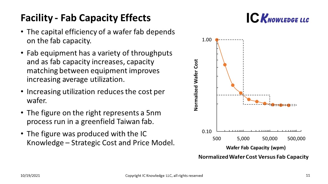
Figure 1. Wafer cost versus fab capacity.
The country a fab is in also impacts the cost. Figure 2 compares the same fab described above designed for 40,000 wafers per month in six different countries. The costs in figure 2 are operating costs only and do not include any incentives.
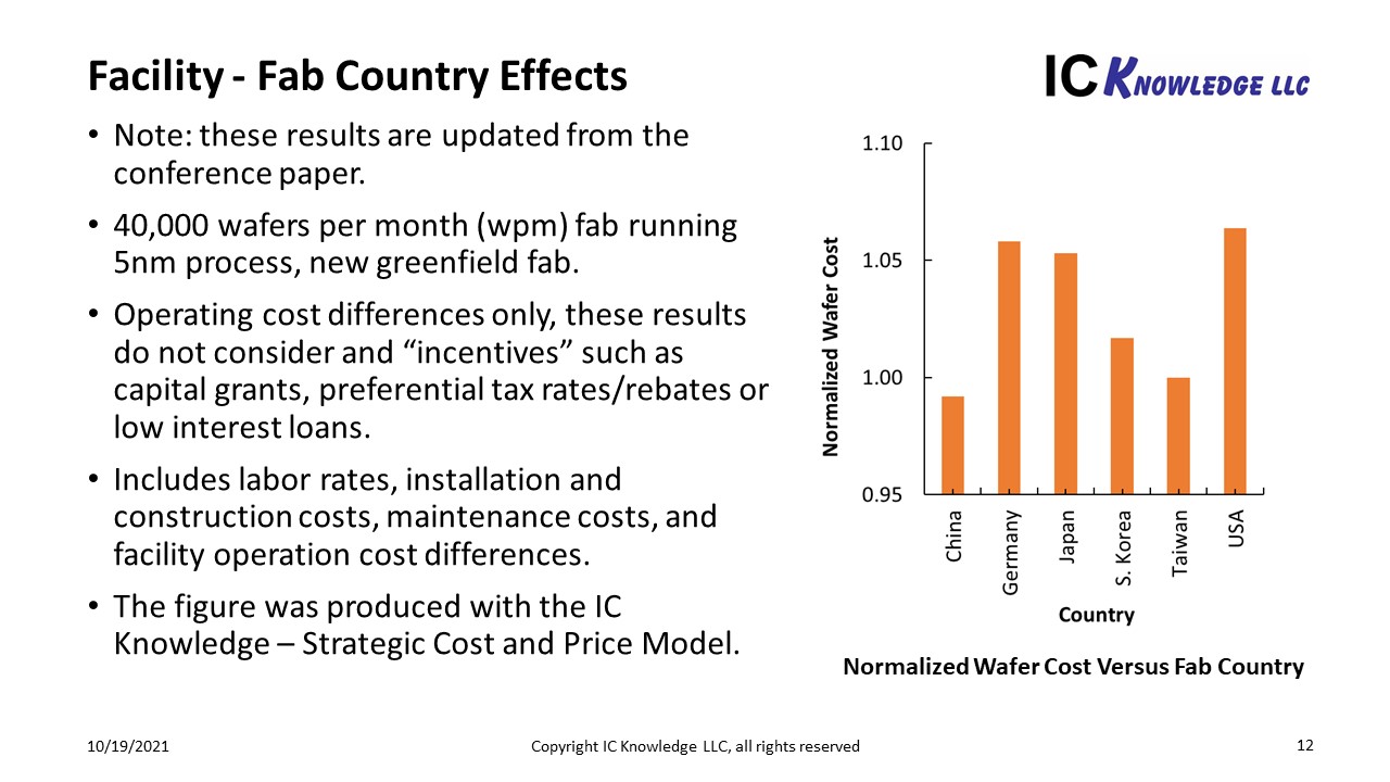
Figure 2. Wafer cost versus country.
Another critical cost factor is the age of the fab. For a new fab depreciation can represent over 60% of the cost of making a wafer. Figure 3 illustrates the same fab previously described for five different time frames:
- the first year ramping up (assuming 50% utilization on average).
- Years two through five when the fab is ramped up but the equipment is still depreciating.
- Year six when the equipment is depreciated.
- Year eleven when the facility systems are depreciated.
- Year sixteen when the building shell is depreciated.
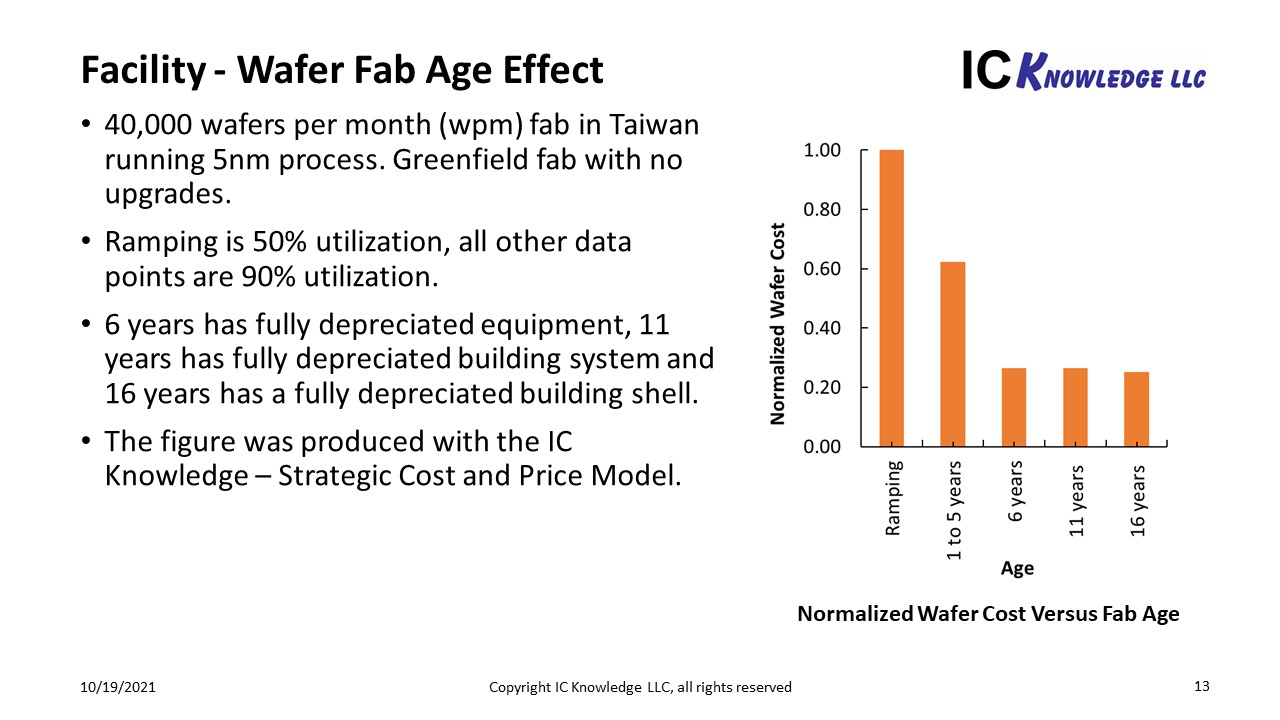
Figure 3. Wafer cost versus fab age.
Accurate cost modeling requires the ability to define the fab capacity, country, and age.
Process Cost
Process costs begin with the starting wafer or wafers cost. Modeling needs to account for whether the starting wafer is a polished wafer, Epi wafer, or specialty wafer such as some kind of SOI. Also modeling needs to allow for more than one wafer, for example for processes where two wafers may be used and then bonded together.
Direct labor costs are the cost for operators to process the wafers. In current generation 300mm fabs there are every few operators because the wafer transport systems lower the front opening unified pods (FOUPs) right onto the tool but there are some operators. The labor hours required for a particular flow most be calculated, and the appropriate labor rate applied depending on the country where the fab is located.
Depreciation is the largest single cost in wafer fabrication, for new processes representing over 60% of the wafer cost (see figure 6 below). Accurate depreciation estimates require determining the equipment required and throughput for every step in the process flow. An accurate model needs to determine the appropriate generation of equipment for a process, the throughput, equipment cost, and physical space needed for the equipment and building a complete set for a target capacity. An accurate model should have background tables of equipment cost and configuration by node and construction costs for cleanroom space to enable detailed capital cost calculations.
Equipment maintenance costs include the costs for equipment parts that are consumed during processing such as quartz rings used in etch chambers, repair parts to replace equipment sub systems that break during operation of the equipment, and finally equipment service contracts. All these costs need to be estimated for the equipment set determined during the depreciation calculations.
Indirect labor costs encompass engineers and technicians that maintain the process and equipment, supervisors that manage the direct labor and managers that oversee everything. Headcounts need to be estimated and salaries by country and year applied.
Facility costs include electricity, water and sewer, ultrapure water generation, natural gas, facility maintenance, occupancy costs and insurance. Many of these costs depend on the country as well as year. An accurate model needs to have background tables by country and year and algorithms to perform the calculations.
Consumables are made up of hundreds of different materials consumed by the process (these are distinct from the equipment parts consumed during processing accounted for in equipment maintenance). Process materials include things like bulk gases, CVD and ALD precursors, CMP consumables, PVD targets, photoresist and reticles and many other items. An accurate model needs to have costs by year for thousands of target materials by year and calculate material usage by process step.
Commercial Implementation
IC Knowledge is the world leader and cost and price modeling for semiconductors and has recently developed process simulation technology to enable step by step process definition and cost estimation (Cost Explorer). Synopsys is a world leader in TCAD tools for technology development and simulation. IC Knowledge and Synopsys have partnered to embed IC Knowledge’s Cost Explorer in Synopsys Process Explorer tool that is used to simulate the physical structure produced by target process flow. Cost Explorer plug in for Process Explorer will enable users of Synopsys DTCO suite to define PPAC targets and design processes to meet those targets in a virtual environment utilizing designed experiments to optimize for all four elements of PPAC simultaneously.
Figure 4 illustrates the IC Knowledge – Synopsys solution.
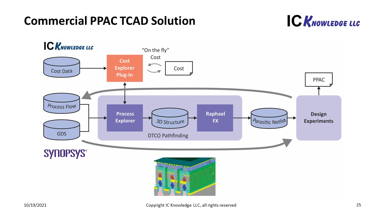
Figure 4. Commercial PPAC TCAD Solution.
The current timeline for this solution:
- Current status – beta testing at one customer with customer developed script to automatically populate Cost Explorer from Process Explorer. Beginning to show the capability to select customers.
- End of 2021 – external cost model with script (Synopsys script) to populate Cost Explorer from Process Explorer.
- Mid 2022 – fully implemented Process Explorer plug-in and commercial availability.
Customer Examples
As mentioned in the previous section we have customer beta testing the solution. The customer is a large OEM who uses Synopsys’ DTCO solution for technology development. The customer is developing Complementary FET (CFET) processes as a next generation solution beyond FinFETs and Horizontal Nanosheets (HNS).
Figure 5 illustrates the wafer cost broken out by category for a possible process flow. In the actual model the results are all in dollars and represent a specific fab and process configuration.
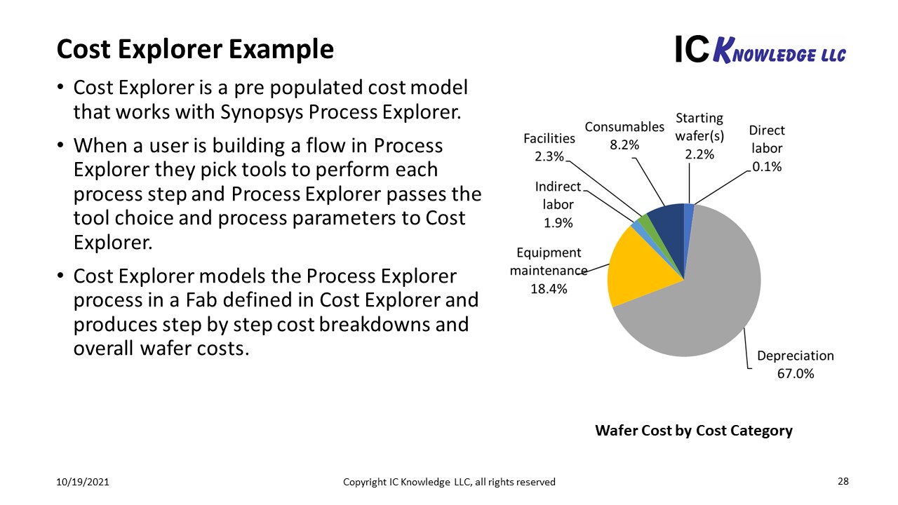
Figure 5. Wafer Cost by Category.
The OEM wanted to evaluate how CFET costs compared to FinFETs. They compared a standard FinFET, a FinFET with a Buried Power Rail (BPR) (BPR enables better density), a monolithic CFET with BPR and a sequential CFET where the CFET process is split between two wafer that are then bonded together, once again, in the actual model the results are all in dollars.
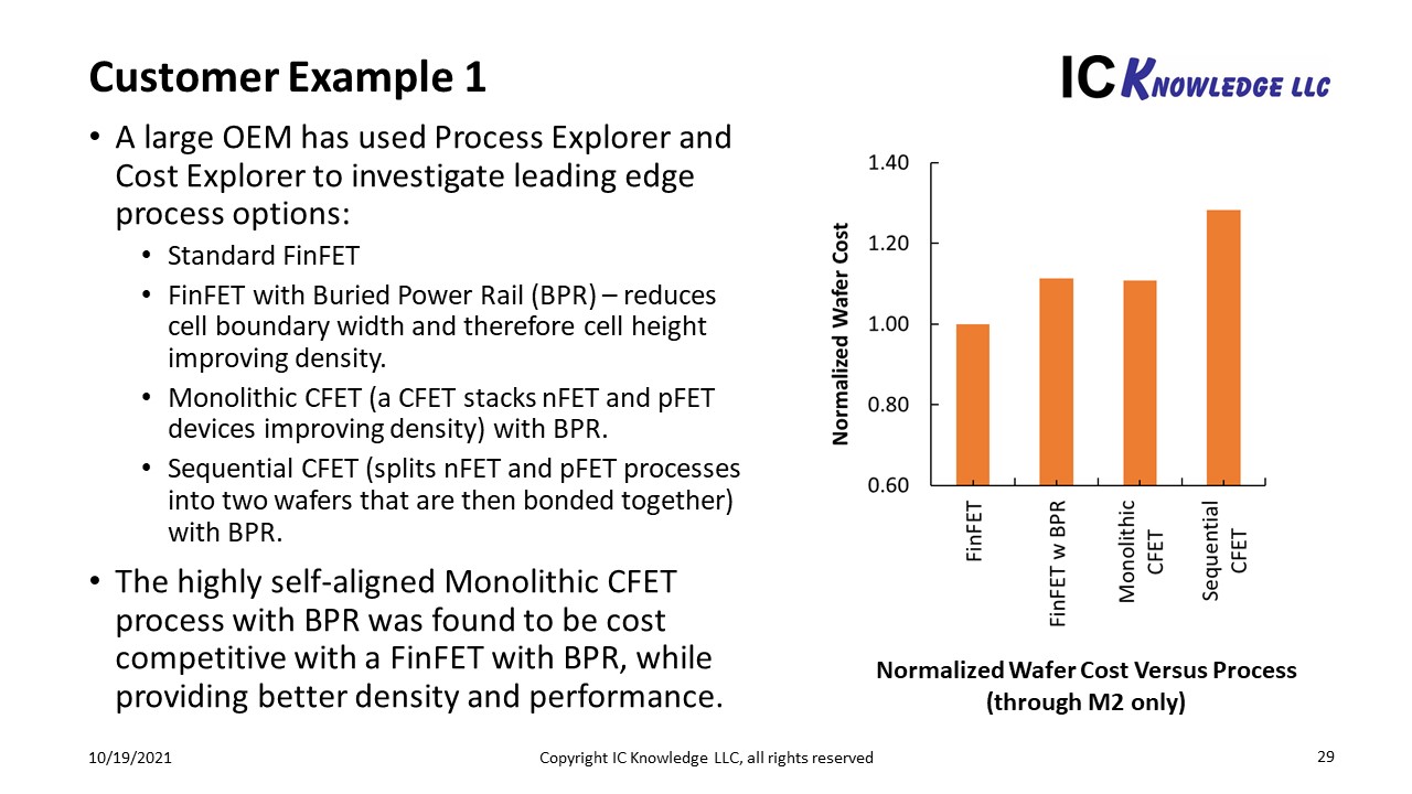
Figure 6. Normalized Wafer Cost Versus Process.
The key conclusion from figure 6 is the OEM developed CFET process with BPR is competitive on cost to a FinFET process with BPR. Because CFETs stack the nFET and pFET devices they offer significant density improvements over FinFETs.
Another conclusion from figure 6 is the monolithic CFET process is less expensive than the sequential CFET process. The monolithic CFET process developed by the OEM is highly self-aligned and cost optimized.
While doing this work the OEM also evaluated lithography options for local interconnect comparing two solutions:
- EUV local interconnect mandrel mask with EUV cut, and EUV via mask.
- EUV local interconnect mandrel mask with multipatterned DUV cut, and EUV via mask.
Because the multipatterned cut can be implemented with a relatively simple multi-patterning scheme they found they could save $52 although there would be some cycle time impact.
Conclusion
The accelerating cost increases to fabricate leading edge wafers are driving the need to switch from PPA based technology development to PPAC based technology development. The partnership of IC Knowledge and Synopsys will for the first time provide the industry with the ability to design for PPAC in a virtual environment before ever running wafers. This capability will be a game changer for the industry and enable the continued evolution of Moore’s law.
References
[1] Geoffrey Yeap of TSMC during Applied Materials IEDM 2019 panel “Logic: EUV is Here , Now What?, “Power Performance Area Cost Time – PPACT where new technologies need to be on-time”.
[2] Luc Van Den Hove, President and CEO of Imec, Imec Technology Forum 2020, “Technologies for People in the New Normal,” slide 45, “Scaling Roadmap” “Power – Performance – Area – Cost”.
[3] Applied Materials, “Selective Gap Fill Announcement,” SEMICON West 2020, slide 2, “Power, Performance, Area-Cost” also including t for time to market.
Also Read:
TSMC Arizona Fab Cost Revisited
VLSI Technology Symposium – Imec Alternate 3D NAND Word Line Materials
Share this post via:


Comments
4 Replies to “SISPAD – Cost Simulations to Enable PPAC Aware Technology Development”
You must register or log in to view/post comments.