

Lithography is arguably the most important step in semiconductor manufacturing. Today’s state-of-the-art EUV scanners are incredibly complex machines that cost as much as a new Boeing jetliner.
From humble beginnings in 1984 as a joint venture with Philips, ASML has grown to become the world’s second largest chip equipment maker – and the only supplier of EUV machines.
“Losing Lithography”, an episode in The Chip Warriors podcast series, provides a first hand account of how the US invented, then lost, this critical part of the chipmaking process. The episode is based on interviews with pioneers at Fairchild Semiconductor, David W Mann Co, Cobilt, GCA, Nikon and Silicon Valley Group (SVG), among others.
Early attempts to print images onto silicon wafers were undertaken at Bell Labs in the mid 1950s. Later that decade, Fairchild improved the process in order to make transistors.
“We decided to use photo resist in order to delineate the areas,” said Jay Last, one of the original eight co-founders of Fairchild, along with Bob Noyce.
“Bell Labs had made some efforts there and thought this was just impossible to work with so they never pursued it. Bob [Noyce] and I worked with Kodak and they gave us the best resists they had at the time and we gradually had a working relationship with them that resists kept steadily improving.
“There were a lot of technical problems and technical setbacks, but we just said we are going to use this and we have to make it work — and we did.”
In the 1960s contact mask aligners were used for wafer printing, with Kulicke & Soffa the first to introduce them commercially. Later, Kasper Instruments became the dominant supplier, but when three former Kasper engineers formed their own company, called Cobilt — and it was acquired by Boston-based CAD giant Computervision in 1972 — a new paradigm for wafer printing emerged.
“Cobilt made mechanical aligners that printed the semiconductor wafer with somewhat superior technology to the standard of the day. And Computervision had a package of automatic alignment which would allow you to align the layers more exactly,” said Sam Harrell, who moved from Computervison to the West Coast to be Cobilt’s vice president of engineering.
“We sold hundreds of machines all over the world. It really reigned until the period of the projection printers became dominant.”
Ed Segal, who sold aligners at Kasper before joining Cobilt, saw how Cobilt lost its lead when Perkin-Elmer developed the projection mask aligner.
“When the mask aligner went to the next stage from a contact mask aligner to what was called a projection aligner, or projecting the image of the mask on the wafer, Perkin-Elmer just absolutely came in and took that market over,” Segal said. “Cobilt attempted to build one and it was really a very big failure. And the company eventually was sold to Applied Materials in 1981.”
Jim Gallagher ran the semiconductor equipment business at GCA, which was the world leader in lithography before ceding the market to Japanese companies in the 1980s. In the podcast, he recounts the eventual demise of the company after Japanese suppliers like Nikon and Canon became market leaders.
“We started to sell off operations as best we could. But when you’re going downhill, so to speak, that’s not the time to start selling because what you’re doing is, everybody knows your problem and they’re going to give the lowest, lowest prices. So that was the beginning of our slide,” Gallagher said.
By the late 1980s, the dominance of Japanese stepper suppliers was a worry for American chipmakers. In an effort to develop an alternative source, Intel worked with Censor, a European company. However, the effort failed and Censor was sold to Perkin-Elmer in 1984.
Intel co-founder Gordon Moore recalls the concern at the time. “The big steppers were coming out of Canon and Nikon. There wasn’t a comparable piece of equipment in the US, and that was such a critical part of the entire process.
“We had a major program with a Liechtenstein company [Censor] to make a stepper. Very sophisticated but also very expensive, and the development went too slowly for them to really make an impact on the market. We ended up buying Japanese equipment because it was the best available, and there wasn’t really an alternative source for that.”
Shoichiro Yoshida, who would later become CEO of Nikon, designed the company’s first step-and-repeat camera for semiconductor manufacturing. In the podcast, hear him describe (in English) the early development of steppers at Nikon.
In the 1990s, SVG expanded into lithography under newly appointed CEO Papken Der Torossian. SVG had tried to buy GCA but the deal never materialized, and GCA was sold to General Signal in 1988.
However, Der Torossian was successful in acquiring a next generation step-and-scan system, Micrascan, developed by Perkin-Elmer in association with IBM — but he said it required tens of millions in R&D and two-and-a-half years to fix bugs in the system. The result was the Micrascan II.
“The machine that they had didn’t work — had a mean time between failure of less than one hour. IBM couldn’t use it. But it had very good basic technology,” he said.
Der Torrossian explains how a shortage of cash led to a missed opportunity to keep advanced lithography in the US.
“In ‘92 ASML was bleeding. Philips owned them and came to me to buy ASML for $60 million. I didn’t have $60 million. I told them, ‘I’ll give you equal number of shares so let’s have a joint venture.’ They said, ‘No, Philips needs cash.’”
By 2001, ASML had turned the business around and it ended up buying SVG — the last major US lithography company — for $1.6 billion. The deal was delayed by several months over national security concerns but eventually approved by the George W. Bush administration after ASML agreed to divest SVG’s Tinsley Labs unit.
The Chip Warriors podcast series, written and produced by Craig Addison, is based on SEMI oral history interviews he conducted between 2004 and 2008. The interviews have been used under license from SEMI, which is not affiliated with the podcast.

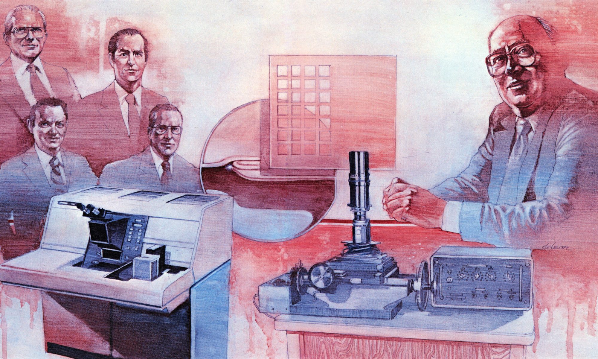
Lithography pioneers are depicted in this painting commissioned by SEMI in 1980. From left, the team behind Perkin-Elmer’s projection mask aligner (Abe Offner, Jere Buckley, David Markel and Harold Hemstreet), and on the right, Burt Wheeler, principal inventor of the photo repeater at David W. Mann Co.
Share this post via:


The Packaging PDK Is the Missing Layer for Co-Packaged Optics