
A recent educational virtual event with the above title was jointly sponsored by Synopsys and Global Foundries. The objective was to bring awareness to state-of-the-art mixed-signal design practices for automotive circuits. The 2-day event comprised of lectures delivered by engineering professors and doctoral students from Wayne State University. The lecture series focused on designing a time interleaved ADC for 5G V2X automotive applications.
If you were not available to attend the live virtual event, you can now listen to the lectures on-demand. This blog provides a backdrop for the lecture series and a brief overview of the lectures.
Automotive Industry
The automotive industry ecosystem has been working on a vehicle-to-everything (V2X) communication system to support autonomous vehicles. The primary purpose of a V2X system is to improve road safety, enhance road traffic efficiency and bring energy savings to automobiles. As such, in addition to the usual requirements of performance, power, area and cost, field reliability of the implemented integrated circuits becomes imperative. As a result, IC designers must ensure that their designs are fail-operational, have low defect rates, and operate reliably over a long period of time.
Lectures Series Overview
You will learn how to design and verify a time-interleaved ADC targeted for 5G V2X application using Global Foundries 22nm FDSOI process technology. You will also learn about the Global Foundries FDSOI process technology. This is the process technology that is used to implement the ADC during this analog-mixed-signal (AMS) lecture series. The lectures cover radio transceiver architecture for V2X systems, ADC architecture, ADC design and related challenges, layout and related changes, accounting for post-layout parasitics, and aging effects.
Why Focus on Time Interleaved SAR ADC?
A complete V2X communication system has four subsystems to it, namely, vehicle-to-vehicle (V2V), vehicle-to-infrastructure (V2I), vehicle-to-pedestrian (V2P) and vehicle-to-network (V2N) communications. The complete system requires transceivers with two different specifications. This would lead to high cost and large chip area to implement the system and will also consume a high amount of power. The WINCAS Research Center at Wayne State University was already working on a single transceiver that can support all V2X applications.
The transceiver architecture is based on frequency planning and programmable ADCs. This means that the ADC has to deal with two different channel bandwidths. For V2V/V2P/V2I, the ADC input bandwidth is 75MHz with sampling frequency at 150MHz. For V2N, the ADC input bandwidth is 400MHz with sampling at 800MHz.
This frequency planning approach offers many benefits, some of which are:
-
- maximum hardware sharing while covering all bands of V2X
- PLLs achieving good phase noise at much reduced current consumption
While the benefits are very attractive, the architecture is the first of its kind, bringing with it its share of challenges to overcome. The ADC plays a critical role in this architecture, making it a suitable circuit to showcase state-of-the-art AMS circuit techniques through a lecture series.
Time Interleaved SAR ADC
The Time Interleaved ADC designed during this lecture series uses 8 channels. Each channel is a SAR ADC. Each SAR ADC has a DAC inside which has a comparator and track and hold. Before diving into the ADC design, the lectures present an improved version of track and hold circuit to avoid the typical issues with traditional implementations. Conventional implementations of track and hold circuits could lead to breakdowns due to over stress voltage conditions. They could also lead to incorrect bit conversions as a result of voltage changes on the top plate of the DAC inside the comparators. The lectures also discuss selection of capacitors for the DAC in order to handle thermal noise.
Design and Layout Challenges
Time Interleaved SAR ADCs are exposed to common mode noise and are sensitive to many types of errors. One such error is the clock skew error. The lecture discusses how to mitigate time skew through the use of dummy logic circuits and offers design techniques to eliminate common mode noise.
AMS designs experience noisy interaction between digital and analog portions of the circuitry. Major sources of this noise are capacitive coupling and power supply lines. Another source is lateral coupling between metal lines that run parallel. Floor plan techniques are presented to help minimize these kinds of situations during the physical routing.
Robustness of SAR ADC
Process, temperature and voltage (PVT) do affect the performance of an ADC. Given this circuit is for an automotive application, validating the design robustness across PVT is very critical. Robustness of a circuit in this regard means that it has a high probability of operating correctly even under conditions outside the specification. Results of corners simulations are presented showing that the performance of the SAR ADC is robust across all corners at different temperatures to meet the AEC-Q100 Grade 1 standard.
Aging and Electromigration
Aging and electromigration triggered faults are very key concerns for automotive applications. The choice of FD-SOI process for implementing the SAR ADC seems to be a good one in this regard. Not only does this process offer FinFET like performance with energy efficiency, it also allows for electrostatic control of the channel via body biasing. This allows for compensating for the static process variations and the dynamic temperature and aging variations.
FD-SOI is the only process technology to bring together three substantial characteristics of CMOS transistors:
- 2D planar transistor structure
- Fully depleted operation
- Capability to dynamically modify the threshold voltage of transistors after manufacturing
Summary
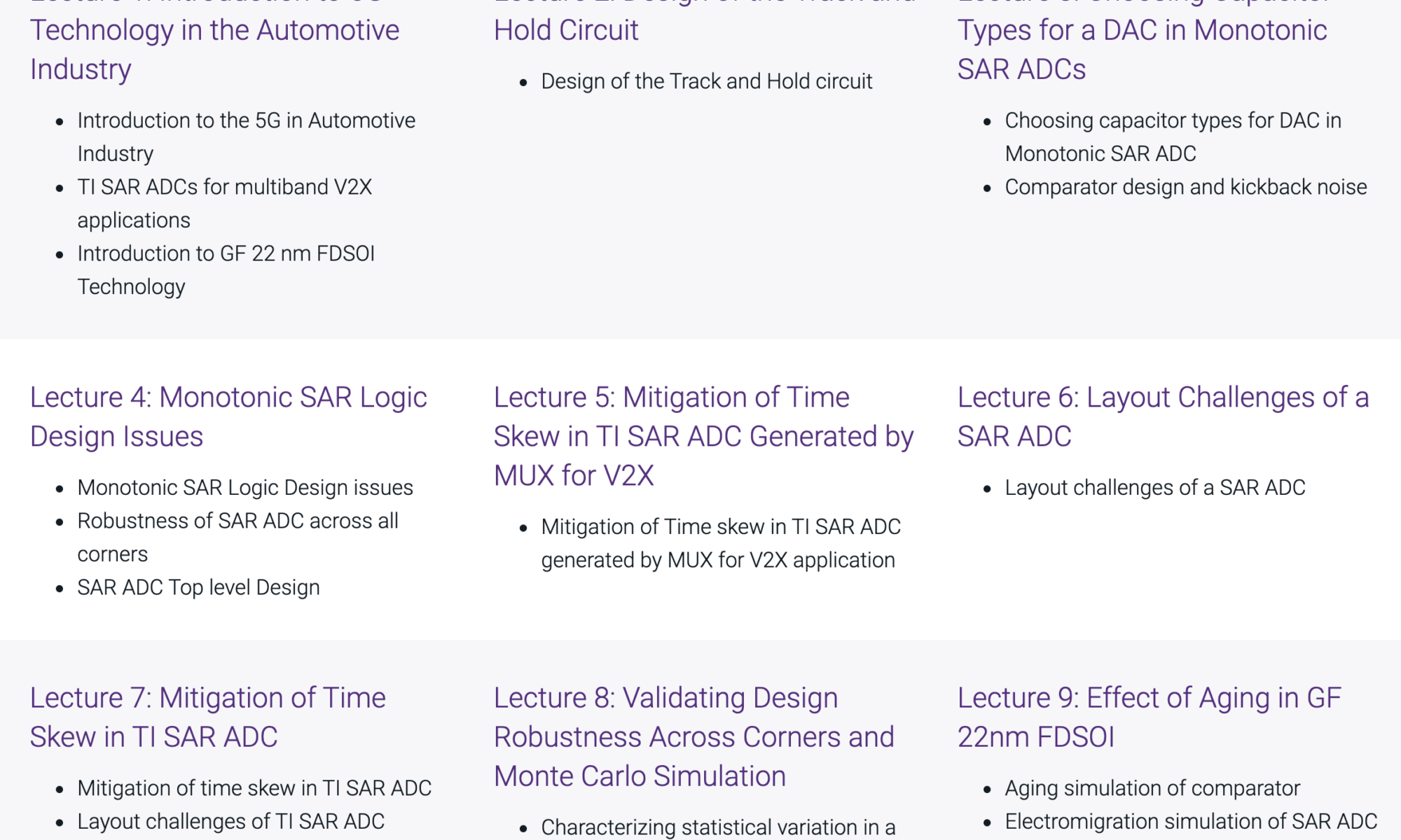
It may be worthwhile for anyone involved in the development of V2X systems to register and listen to these lectures to learn some new circuit techniques. Below is a screenshot showing the different topics covered over a series of nine lectures. You can listen to the lectures in any order or just the ones that are of interest to you. Access the lecture series on-demand from here.

Also read:
Synopsys’ ARC® DSP IP for Low-Power Embedded Applications
Synopsys’ Complete 800G Ethernet Solutions
Safety + Security for Automotive SoCs with ASIL B Compliant tRoot HSMs
Share this post via:


Comments
There are no comments yet.
You must register or log in to view/post comments.