
Standard Cell Scaling
Complex logic designs are built up from standard cells, in order to continue to scale logic we need to continually shrink the size of standard cells.
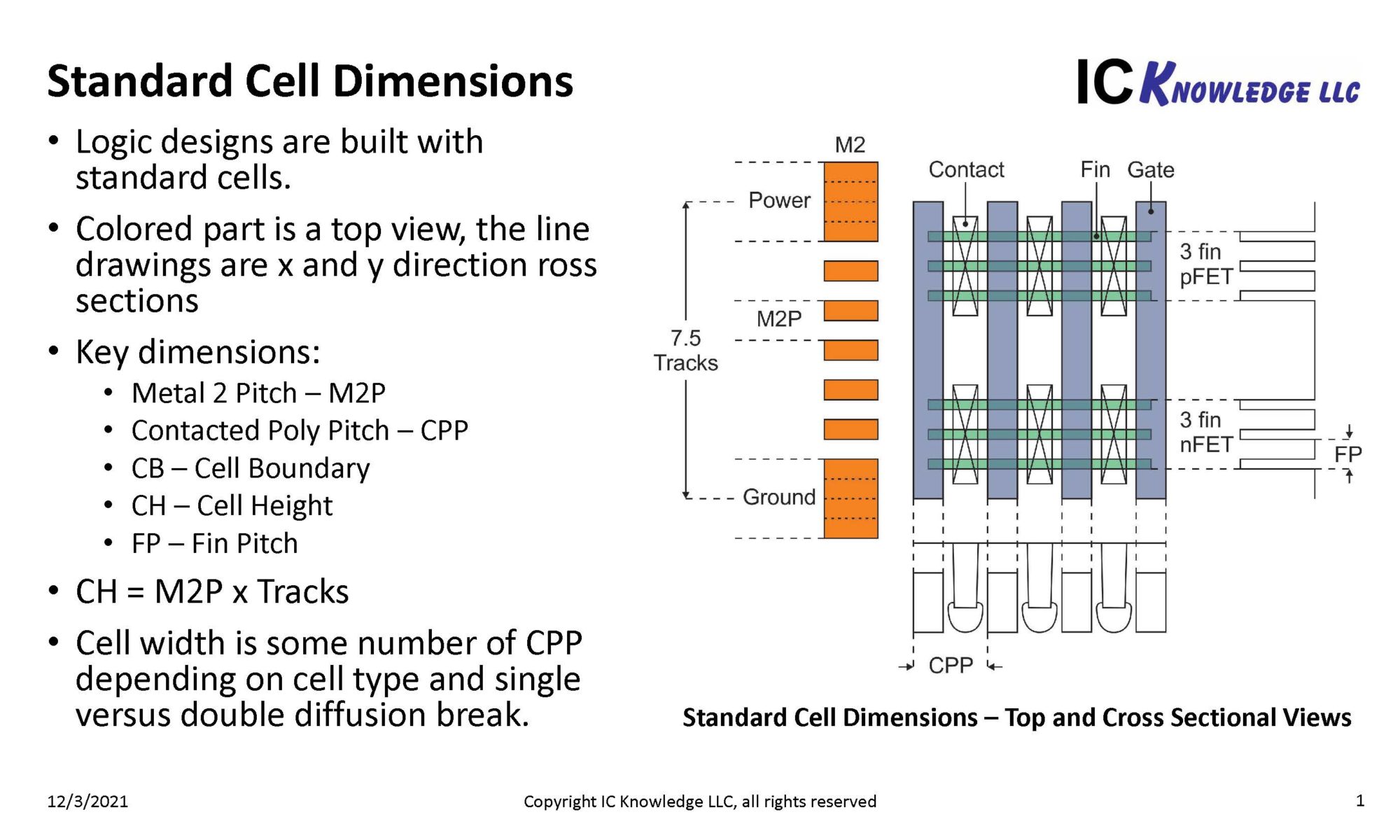
Figure 1 illustrates the dimensions of a standard cell.

Figure 1. Standard Cell Dimensions.
From figure 1 we can see that shrinking standard cell sizes requires shrinking the cell height, or the cell width, or both. The height of the cell is Metal 2 Pitch (M2P) multiplied by the number of Tracks. The cell width is determined by the Contacted Poly Pitch (CPP) and whether the cell has single or double diffusion breaks.
Shrinking cell height and width impacts the underlying device structures. In figure 1 on the right side is a simple cross section of the fins that must fit in the cell and at the bottom of the figure is a simple cross section of the elements that make up CPP. The two Intel papers I want to discuss in this write-up are the 3-D CMOS paper that can enable reduced cell height and the 2D Monolayer CMOS paper that can enable reduced cell width.
3-D CMOS (CFET)
Figure 2 illustrates the FinFET device dimensions that must fit into the cell height.

Figure 2. Cell Height Scaling.
From figure 2 we can see that the cell height includes two cell boundaries, some number of fin pitches (depends on number of fins) and the n-p spacing between the nFET and pFET fins.
Figure 3 illustrate that once a transition is made to horizonal nanosheets the n-p spacing can be reduced by various options.

Figure 3. n-p Spacing.
On the left side of figure 3 is a standard horizontal nanosheet that needs the same n-p spacing we would see with a FinFET. This type of configuration supports a 6-track cell height or with the addition of buried power rails (BPR), a 5-track cell (BPR reduce the cell boundary width). The middle of the figure illustrates adding a dielectric wall in between the nFET and pFET to reduce n-p spacing and enable track heights of 4.33 to 4.00. Finally on the right side of the figure a 3-D CMOS device (CFET), is illustrated and the n-p spacing is now zero in the lateral dimension because the FETs are stacked, this approach can support tracks heights of 4.00 to 3.00.
In their “Opportunities in 3-D stacked CMOS transistors” paper at IEDM, Intel provided an overview of 3D-CMOS.
The basic idea behind 3D-CMOS is illustrated on the left side of figure 4.

Figure 4. 3D-CMOS.
There are two main options for 3D-CMOS.
In a sequential approach the bottom device layer is fabricated up through gates and contacts on one wafer, a top layer of devices is separately fabricated on a second wafer and then deposited onto the bottom devices through layer transfer or bonding, followed by interconnect for the resulting two-layer structure. The sequential approach is illustrated in the top right-hand side of figure 4.
The sequential approach requires extra processing because the bottom and top layers are fabricated independently, but it offers the ability to mix and match various materials, for example Germanium PMOS devices with Silicon NMOS devices or even introducing Gallium Nitride devices. It does require combining the two device layers without degrading either layer and a critical bonding step.
The second approach is the self-aligned approach, where both the bottom and top layers are fabricated on the same wafer. This approach can in theory reduce the process complexity but does present integration challenges to achieving good device performance for both layers. The self-aligned approach is illustrated in the bottom right-hand side of figure 4.
3D-CMOS is a promising solution to continue scaling after horizontal nanosheets enter production.
2D Monolayer CMOS
If we look at the CPP cross section at the bottom of figure 1 in more detail, we get the diagram on the left side of figure 5. CPP is made up of Gate Length (Lg), contact width and twice the contact to gate spacer thickness.

Figure 5. Contacted Poly Pitch Scaling.
As we can see from the table on the right side of figure 5, TSMC for example, has been shrinking CPP by reducing all three dimensions.
With respect to Lg it is limited by the type of device being used. The more constrained the channel is and more gates that are used to control the channel, the shorter the minimum gate length can be. Figure 6 presents the limits for different device types and presents the minimum gate length versus channel thickness and number of gates for silicon.

Figure 6. Gate Length Scaling.
From the bottom left part of figure 6 we can see that for a planar transistor with a single gate, the channel is poorly controlled, and the gate length limit is around 30nm (theoretically it is less, but all the logic manufacturers moved off single gate planar devices by 30nm). Moving to a planar device with a thin channel and two gates as is seen with FDSOI, reduces the minimum channel length to approximately 23nm. FinFETs with the channel constrained to a thin fin and three gates enables gate lengths down to approximately 16nm, this is one of the reasons FinFETs have been adopted as the logic mainstream. As we move forward horizontal nanowire/nanosheets with four gates offer minimum gate lengths of approximately 13nm. Finally, beyond nanosheets, the Intel work discussed here addresses 2D devices that can enable channels of less than 10nm providing further CPP scaling. This is a promising next step beyond 3D-CMOS or may be integrated with 3D-CMOS. There were many papers presented at the conference representing a variety of companies and research groups illustrating the interest in this technology.
The Intel paper discussing this is entitled: “Advancing 2D Monolayer CMOS Through Contact, Channel and Interface Engineering”.
As silicon is scaled down, the channel thickness must get thinner and mobility degradation eventually occurs, the silicon limit for good mobility is approximately 5nm. Transition Metal Dichalcogenide (TMD) materials show similar mobility in monolayer films ~1nm to their bulk mobility making them attractive candidates for 2D devices. TMD films will have lower mobility and higher contact resistance than current generation silicon CMOS devices, but simulations indicate that even with these draw backs, stacking enough 2D layers will provide a performance and scaling improvement over silicon horizontal nanosheets, for example with if 2D layers are stacked 6 high with a Lg of 5nm and metallic contacts, significant scaling, power, and performance improvements can be achieved.
Figure 7 illustrates 2D Devices.

Figure 7. 2D Devices.
The paper reviews three key areas: channel material quality, contact resistance, and gate stack quality.
The best channel results in literature are from deposition techniques that haven’t been demonstrated on 300mm wafers. MOCVD and nucleated CVD on pre patterned seeds have the potential for 300mm deposition. MOCVD offers the prospect of a wide temperature range including 300oC deposition that could open up TMD channel deposition compatible with the Back End of Line (BEOL). Nucleated CVD offers grain boundary free devices and Intel has achieved the best published WS2 mobility.
Low contact resistance contacts to NMOS and PMOS remain a challenge for 2D FETs. The authors show promising results for Sb on MoSi2, and Sb offers a higher melting point than Bi (the other leading NMOS contact material). PMOS contacts remain far more challenging, once again the authors showed some results with Ru but there are still a lot of challenges.
The 2D materials of interest here are well known to collect organic processing residues that can inhibit ALD deposition of gate oxides. The authors compared a vacuum anneal and a forming gas anneal, and both reduced the carbon contamination levels, the forming gas anneal was shown to improve measured electrical performance for a MOSCAP.
By comparing the work done here with previously published work the authors have shown where 2D devices currently stand and introduced promising new contact materials and deposition techniques.
2D devices are far from being ready for manufacturing but several groups are pursuing them, and steady progress is being made.
Conclusion
Samsung is currently trying to be the first in the industry to put horizontal nanosheets (HNS) into production. Intel and TSMC are also working on HNS. It is likely that HNS will carry the industry at least through 2025. By around 2028 3D-CMOS (called CFETs by others) may be ready for production incorporating vertical stacks of n and p nanosheets. As a follow on to 3D-CMOS or even and extension of 3D-CMOS 2D devices are a potential path for continued scaling past the end of the decade. Intel is clearly trying to reassert themselves as a semiconductor technology leader.
Also Read:
SISPAD – Cost Simulations to Enable PPAC Aware Technology Development
TSMC Arizona Fab Cost Revisited
Share this post via:


Comments
5 Replies to “Intel Discusses Scaling Innovations at IEDM”
You must register or log in to view/post comments.