You are currently viewing SemiWiki as a guest which gives you limited access to the site. To view blog comments and experience other SemiWiki features you must be a registered member. Registration is fast, simple, and absolutely free so please,
join our community today!
1. Why the substrate matters
Every transistor sits in, or on, a few hundred nanometres of crystal; the rest of the wafer is mechanical support and, often, a liability. Silicon won because it combines a moderate bandgap (1.12 eV), a native oxide (SiO2) of excellent quality, and the ability to be grown as near-perfect single crystals… Read More
Intel’s 18A process technology has become one of the most scrutinized semiconductor manufacturing nodes in the industry. It represents Intel’s introduction of two major innovations: RibbonFET gate-all-around (GAA) transistors and PowerVia backside power delivery (BSPD). These technologies are intended to improve transistor… Read More
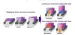
The transition from FinFET to Gate-All-Around (GAA) transistor technology represents a pivotal moment in the evolution of logic devices, driven by both physical scaling limits and the rapidly growing computational demands of artificial intelligence. As semiconductor technology approaches the sub-3 nm regime, traditional… Read More
Scott Bibaud has served as President, Chief Executive Officer and a director since October 2015. Mr. Bibaud has been active in the semiconductor industry for over 25 years. He has successfully built a number of businesses in his career which grew to generate over $1 Billion in revenue at some of the world’s largest semiconductor… Read More
In the early 2000s, Moore’s Law—the observation that the number of transistors on a chip doubles roughly every two years—was facing an existential crisis. As semiconductor nodes shrank below 90nm, planar transistors suffered from debilitating issues: leakage currents soared, power efficiency plummeted, and scaling became… Read More
By Nir Sever, Senior Director Business Development, proteanTecs
Silicon-proven LVTS for 2nm: a new era of accuracy and integration in thermal monitoring
Effective thermal management is crucial to prevent overheating and optimize performance in modern SoCs. Inadequate temperature control due to inaccurate thermal sensing… Read More
Transistor fabrication has spanned the gamut from planar devices o FinFET to Gate-All-Around (GAA) as silicon dimensions have decreased in the quest for higher density, faster speeds and lower power. Process development engineers use powerful simulation tools to predict and even optimize transistor performance for GAA devices.… Read More
Alchip Technologies Ltd., a global leader in high-performance computing (HPC) and artificial intelligence (AI) ASIC design and production services, continues its trajectory of rapid growth and technical leadership by pushing the boundaries of advanced-node silicon, expanding its global design capabilities, and building… Read More
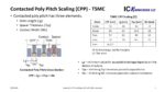
TSMC presented two papers on 3nm at the 2022 IEDM; “Critical Process features Enabling Aggressive Contacted Gate Pitch Scaling for 3nm CMOS Technology and Beyond” and “A 3nm CMOS FinFlexTM Platform Technology with Enhanced Power Efficiency and Performance for Mobile SOC and High Performance Computing Applications”.
When … Read More
Intel recently released an exceptional video providing an insightful chronology of MOS transistor technology. Evolution of Transistor Innovation is a five-minute audiovisual adventure, spanning 50 years of Moore’s Law. Some of the highlights are summarized below, with a few screen shot captures – the full video is definitely… Read More