
Last Thursday Intel held their investors meeting, in this write up I wanted to focus on my areas of coverage/expertise, process technology and manufacturing.
Technology Development presented by Ann Kelleher
Last year Intel presented their Intel Accelerated plan and, in this meeting, we got a review of where Intel stands on that roadmap.
Intel is targeting performance per watt parity with the foundries in 2024 and leadership in 2025. This is something I am following very closely, I was due to present “Logic Leadership 2025” at the ISS conference in January but the conference is now delayed to the beginning of April. I am doing a deep dive comparison of Intel, Samsung and TSMC process technology through 2025 in that presentation, not wanting to preempt myself I am not going to cover that material here other than to say if Intel hits these goals, they will be competitive.
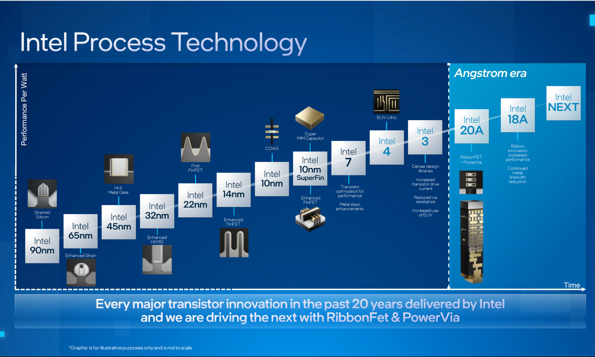
Figure 1 presents a slide from the presentation talking about Intel’s history of innovation. Intel claims that every major transistor innovation for 20 years has been delivered by Intel. I would agree that has been true until recently but at 5nm TSMC introduced SiGe FinFET fin and at 3nm Samsung is currently ramping the first Horizontal Nanosheet (HNS) devices. When Intel introduces their RibbonFET HNS they will be at one to two years behind Samsung. Intel does appear to be leading the backside power delivery race.

Figure 1. Process Technology Innovations.
It was interesting to hear that they are putting a focus on predictable execution and modular development. They are working more with equipment suppliers and adopting industry best known methods. In my opinion these are all good moves on Intel’s part. For too long Intel has missed out on developments done outside of the company that were readily available to others from the equipment suppliers.
Figure 2 presents Intel’s EUV roadmap.

Figure 2. EUV Roadmap.
Two comments on this figure, originally the 18A process node was due in 2025 and I expected it would be the first High-NA EUV node, but it is now planned for the second half of 2024 and will be manufactured with 0.33NA EUV.
My second comment is that Intel is making a lot of the fact that they are due to get the first High-NA EUV tool and they are presenting this as a competitive advantage. What I have heard is that Intel gets the first High-NA tool but TSMC gets the second roughly a month later, that doesn’t strike me as a significant advantage.
Figure 3 presents the future process progression from 4 to 3 to 20A to 18A. I thought it was funny to see the graphic is of FinFETs for 20A and 18A when they are HNS processes. Its not really important as it is just for illustration purposes but I noticed it.

Figure 3. Future Nodes.
Intel is targeting five “nodes” in 4 years, a pace that is faster than we have seen from anyone in the industry in the past and a huge acceleration for a company that took 3 years for the 14nm node and 5 years for the 10nm node.
- 7nm – Intel’s original 10nm process ramped in 2019, they then developed the 10+ or super fin node and now have the enhanced Super Fin node they have renamed 7nm. I agree this is an appropriate renaming as the density and performance are similar to the foundry 7nm nodes. 7nm delivers a 10% performance per watt boost over the 10 Super Fin through more strain and lower resistance for faster channels and better routing. 7 entered production in early 2022.
- 4nm – originally referred to as 7nm, I pointed out some time ago that based on the 2x density improvement Intel was expecting it would be like a foundry 4nm process and they have now renamed it 4nm. It is interesting to me that they are no longer talking about a specific number for the density change making me wonder if it will be less dense than originally expected. The current quote is “significant density jump”. The process will deliver a 20% performance per watt improvement versus 7nm and be Intel’s first use of EUV and is due in the second half of 2022.
- 3nm – I view this as kind of a half-node such as the foundries often do, it will have denser libraries, an optimized metal stack with less via resistance, more EUV use and provide an 18% performance per watt improvement. It is due in the second half of 2023.
- 20A (A for angstrom, this is equivalent to 2nm) will be a HNS (Intel calls this RibbonFET) and Backside Power Delivery (Intel calls this PowerVia). This process is expected to provide a 15% performance per watt improvement and is due in the first half of 2024. I am surprised that the performance doesn’t take a bigger jump with the new transistor type and BPD, Samsung is claiming a 35% jump for their FinFET to HNS transition (although Samsung’s 5nm process wasn’t a very strong offering so 3nm being a lot better is less impressive than it might otherwise be).
- 18A – I view this as another half-node, it will offer a 10% performance per watt improvement, smaller linewidths and is due in the second half of 2024. This was originally expected in early 2025 and Dr. Kelleher said they have already delivered an 18A test chip to a customer, they expect 2 tape outs in 2022 and 4 test chips in the first half of 2023. It surprises me that they have silicon they are showing customers this early.
This is an incredibly aggressive roadmap and from everything presented it sounds like Intel is on or ahead of schedule, that is a great achievement.
I am not going to discuss Intel’s packaging technology here but they do have an impressive portfolio in that area.
Manufacturing was presented by Keyvan Esfarjani
Intel is investing to accelerate new nodes and grow scale. They are leveraging their advanced packaging and “world class supply chain”.
Figure 4 illustrates Intel’s planned five nodes in four years on the left side, scale in the middle, and global footprint on the right.

Figure 4. Intel Manufacturing Strategy.
In the talk it was mentioned that Intel would roughly double their “manufacturing footprint” by 2026. I am not sure what that means exactly, the middle of figure doesn’t show a doubling of wafers starts so they presumably mean the number of transistors produced that is a product of additional wafer starts and node shrinks.
On the right side of the figure both fabs and packaging facilities are shown, a few comments on the fabs:
- Oregon is home to Intel’s R&D facilities and also some production. Fabs RP1, DC1 + Fab 15 expansion, D1D, D1X, D1X phase 2 and phase 3 are all there. D1C/15 and D1D are former development fabs used for production now. The various phases of D1X lead the latest generation logic process development and RP1 is research path finding.
- Ireland is home to Fab 24, Fab 24 phase 2 and the new Fab 34. Ireland is a production site.
- New Mexico is transitioning to packaging and is also where 3D XPoint memory is developed. Fabs 11x, 11x phase 2 and 11x 3D are there.
- Arizona is home to Fabs 12C, 32 and 42 and the under construction Fabs 52 and 62. Arizona is a production site.
- Israel is home to Fabs 28, 28 phase 2 and the under construction Fab 38.
- Ohio will be home to two planned new fabs initially with additional fabs in the futures.
- New EU site is under discussion for a multi fab complex.
- Dalian China – not shown, sold to SK Hynix.
Figure 5 illustrates Intel’s “Smart Capital” plan.

Figure 5. Smart Capital.
The left side of the figure shows the time versus investment of the various parts of building a fab. The plan is to build big shells in advance since they are a smaller segment of the cost and take the longest to build, and then fill them with equipment as needed. This has been standard practice at TSMC for a long time and is a good practice to adopt. I should also mention that my data is that it takes Intel significantly more capital to build a fab shell per square meter than anyone else and hopefully they are addressing that as well.
They are also planning to use both internal and external capacity and are seeking government support and customer prepays to help offset capital costs.
Figure 6 illustrates the idea that getting into the foundry business will allow Intel to use their assets longer. From the start I have questioned why Intel wants to get into the foundry business. Intel’s gross margins are over 50%, in the foundry business TSMC as the market leader gets 50% gross margins but everyone else is closer to 25%. As a foundry start up I would expect Intel to have margins around 25% for a very long time. The only thing that made sense to me was getting longer life out of their assets and here they discuss that.
Intel and TSMC both started bringing 300mm fabs on-line for the 130nm node around 2001/2002, Intel’s 130nm, 90nm, 65nm and 45nm capability are long gone, converted to 32nm and smaller nodes. TSMC on the other hand is still running 130nm, 90nm, 65nm and 40nm fabs.

Figure 6. New Operational Model.
Conclusion
A lot of what Intel is doing is adopting best practices from others. The big take away to me is that they appear to have gotten back on track on development and are executing on a roadmap that has the potential to get them back at or near process leadership.
Also read:
Tower Semi Buyout Tips Intel’s Hand
Intel buys Tower – Best way to become foundry is to buy one
The Intel Foundry Ecosystem Explained
Share this post via:


Comments
13 Replies to “Intel 2022 Investor Meeting”
You must register or log in to view/post comments.