Intel recently released an exceptional video providing an insightful chronology of MOS transistor technology. Evolution of Transistor Innovation is a five-minute audiovisual adventure, spanning 50 years of Moore’s Law. Some of the highlights are summarized below, with a few screen shot captures – the full video is definitely worth viewing.
The speaker is 16+ year Intel veteran Marisa Ahmed, a Member of the Technology Leadership Marketing Team. Marissa is responsible for building technology marketing strategies and activities in support of Intel’s process, packaging and manufacturing capabilities.
1971
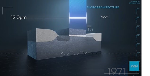
The figure above establishes a baseline for the MOS field effect transistor, circa 1971.
(Note the additional supplemental info provided with the transistor cross-sections that follow – e.g., the total number of transistors released; the number of metal layers for the process generation; the exposing wavelength for lithographic patterning; the wafer size; and, the related Intel product families.)
Polycide and Salicide: 1979-81
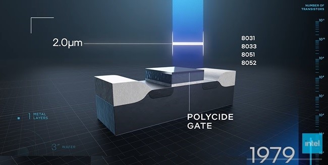
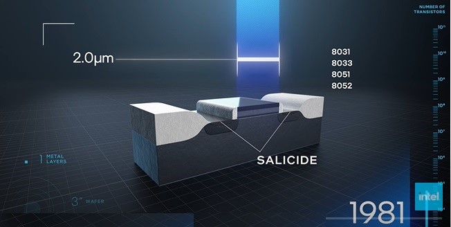
With ongoing Dennard scaling of the device gate length, the sheet resistivity of the polysilicon gate material was increasing. Similarly, the transistor drain/source series resistance (Rs, Rd) was increasing. The contact resistance (Rc) to the metal layer was also increasing, due to the scaling of the S/D junction depth. To address these problematic parasitics, a process innovation emerged to create a silicide. A refractory metal such as Titanium was deposited and alloyed at elevated temperature with the exposed silicon. (Salicide is a composite term for “self-aligned silicide” – the deposited metal does not react with the adjacent dielectric materials.)
STI: 1995
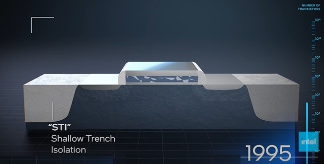
The device electrical isolation and surface topography underwent a significant change, in the transition from local oxidation of silicon (LoCoS) to shallow trench isolation (STI).
LoCoS was a process method where the field oxide isolation between devices was formed by patterning a hard mask over the device area, and exposing the field to an oxidation environment. Oxygen would diffuse from the high-temperature environment through the growing field oxide layer to reach with the silicon crystal at the oxide-substrate interface. The resulting oxide profile was a tapered (“bird’s beak”) surface topography, better for metal traversal between devices.
To facilitate further scaling, a new process for field oxide separation was introduced. STI leveraged major improvements in anisotropic dry etching technology (with near vertical sidewalls) combined with chemical vapor deposition of dielectric materials.
Aluminum à Copper
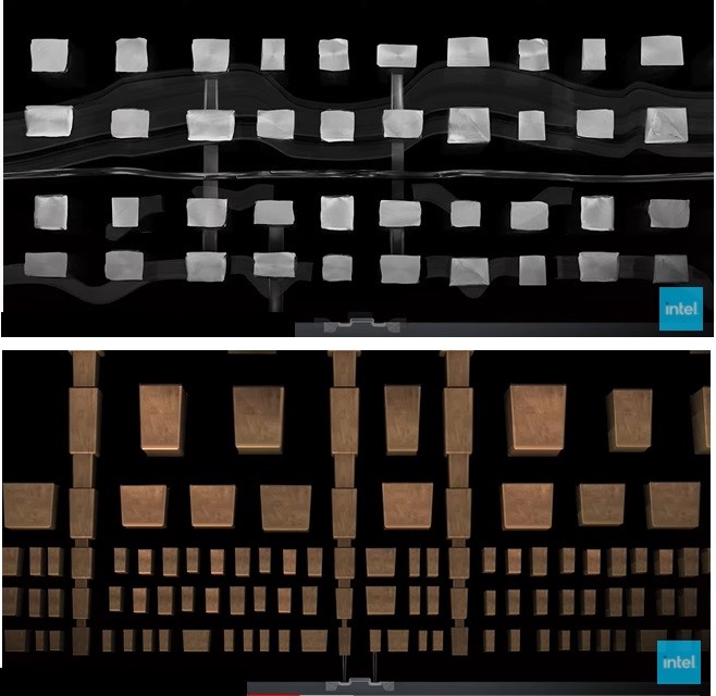
A watershed (non-device) process enhancement in the late 1990s was the transition from Aluminum metallization to Copper. Dennard scaling continued to enable greater device current and lower device capacitances. This era was marked by the transition from gate fanout load-dominated circuit delay to significant contributions from the R*C interconnect delay from the driving gate output to the fanouts. The need for interconnects with improved resistivity and electromigration robustness necessitated the transition from Al to Cu.
Concurrent with that material transition, a major shift in interconnect patterning was required. Aluminum as the primary interconnect involved a rather straightforward deposition, lithography, and subtractive removal process flow. Due to the difficult chemistry associated with dry etching of copper – e.g., corrosive gases, few volatile copper-based reaction products to pump out – a damascene patterning method was required. The dielectric to surround the metal was deposited, a trench was etched in the dielectric (and interlevel dielectric below for the vias), then copper was deposited in the trench through electroplating.
In addition to the additive damascene process replacing the subtractive Al etch method, it was also therefore necessary to evolve the chemical-mechanical polishing (CMP) process step. The wafer surface with the deposited Cu is placed face down onto a polishing pad, which rotates at a low speed. A rotating piston at higher RPM provide an appropriate downward force on the wafer (Newtons/cm**2), and a slurry is introduced onto the pad. The slurry consists of both a chemical solution and a fine grit. The chemical is intended to selectively react with the material to be removed – Cu, in this case – while the mechanical polish removes the result of the reaction. An extremely flat surface topography is produced. As shown in the figure above, as well as the succeeding figures, CMP has enabled a much-needed increase in the number of metal layers available for interconnecting the scaled circuit density.
Gate and gate oxide enhancements
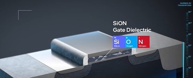
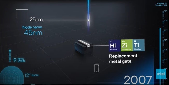
Device evolution encountered issues with continued scaling of the gate oxide thickness. The influence of the input gate electric field on the device channel requires scaling the gate oxide capacitance: Cg ~ ((K*E0)/t), where K is the relative dielectric constant and t is the gate oxide thickness. As the gate oxide became thinner, gate tunneling current through the device input increased. To equivalently increase Cg without the issues of reducing the thickness, alternative high-K dielectric materials replaced SiO2 for the gate oxide.
Scaling the traditional polycrystalline silicon gate material was resulting in higher resistivity and greater sensitivity to non-uniformity in the polySi grain size, distribution, and impurity concentration. A replacement metal gate process step was introduced, displacing polySi as the gate material. (For more info on this rather difficult step, do a follow-on search for high-K, metal gate “HKMG gate-first versus gate-last” process; the term replacement in the figure above refers to a gate-last flow.)
FinFET: 2011
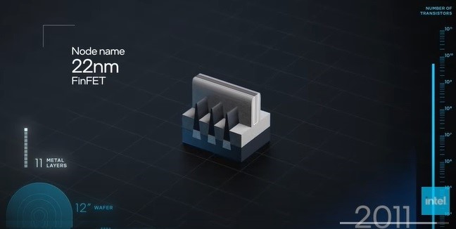
Intel amazed the industry with its aggressive adoption of a new transistor topology at the 22nm process node – the FinFET (also known as the “tri-gate FET”).
The traditional planar S/D channel topology had an increasing issue with (sub-channel) leakage current between source and drain when the device was “off”. To reduce the sub-threshold leakage, a device topology was required where the gate input provided greater electrostatic control over the channel. The vertical channel “fin” has the input gate traversing over the sidewalls and top. In the figure above, a single gate inputs traverses over three silicon fins to be connected in parallel – the channel current flows through the vertical fins. The thickness of the fin is sufficiently small such that the gate input electric field control reduces the sub-threshold leakage substantially, which has enabled much greater battery life for laptop and mobile electronics.
Gate-All Around (GAA) Ribbon FET: Intel 20A in 2024

To further improve the electrostatic gate control over the channel, another major evolution in the transistor topology is emerging to replace the FinFET. A gate-all-around configuration involves a vertical stack of electrically isolated silicon channels. The gate dielectric and gate input utilize an atomic layer deposition (ALD) process flow to surround all channel surfaces in the stack.
Intel will be releasing their GAA Ribbon FET 20A process in 1H 2024.
Summary
The evolution of the field effect transistor over the past 50 years is rather amazing. The figure below illustrates this progress, with the devices drawn to scale.
This evolution was enabled by the innovative ideas and hard work of research and development teams throughout the industry, with expertise ranging from materials science to chemistry to optical lithography to the physical of deposition/etch process steps. Rather incredibly, this progress shows no signs of stopping anytime soon, absolutely.
Also read:
The Intel Foundry Ecosystem Explained
Intel Discusses Scaling Innovations at IEDM
Share this post via:


Comments
13 Replies to “Intel Evolution of Transistor Innovation”
You must register or log in to view/post comments.