You are currently viewing SemiWiki as a guest which gives you limited access to the site. To view blog comments and experience other SemiWiki features you must be a registered member. Registration is fast, simple, and absolutely free so please,
join our community today!
It Isn’t Transistory
There’s a quiet upheaval happening in the semiconductor industry. The rules that have always governed the industry are fraying, undoing assumptions that we took for granted, that was pounded into us in school. The irreproachable Moore’s Law, that exponential progress will make things cheaper, better,… Read More
Kinam Kim is a longtime Samsung technologist who has published many excellent articles over the years. He is now the Chairman of Samsung Electronics, and he gave a very interesting keynote address at IEDM.
He began with some general observations:
The world is experiencing a transformation powered by semiconductors that has been… Read More
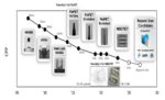
IBM at IEDMby Scotten Jones on 01-10-2022 at 6:00 amCategories: Events
IBM transferred their semiconductor manufacturing to GLOBALFOUNDRIES several years ago but still maintains a multibillion-dollar research facility at Albany Nanotech. IBM is very active at conferences such as IEDM and appears to have a good public relations department because they get a lot of press.
At the Litho Workshop … Read More
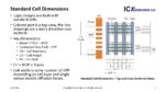
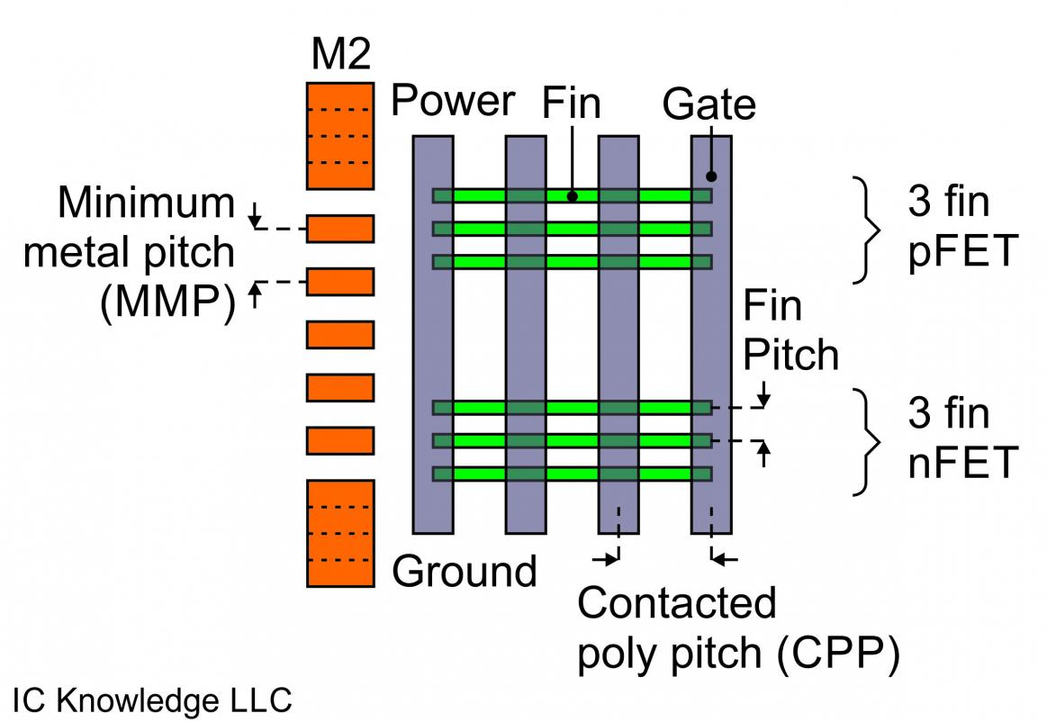
Standard Cell Scaling
Complex logic designs are built up from standard cells, in order to continue to scale logic we need to continually shrink the size of standard cells.
Figure 1 illustrates the dimensions of a standard cell.
Figure 1. Standard Cell Dimensions.
From figure 1 we can see that shrinking standard cell sizes requires… Read More
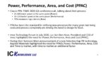
I was asked to give a talk at the 2021 ISS conference and the following is a write up of the talk.
The title of the talk is “Logic Leadership in the PPAC era”.
The talk is broken up into three main sections:
- Background information explaining PPAC and Standard Cells.
- A node-by-node comparisons of companies running leading edge logic
…
Read More
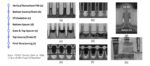
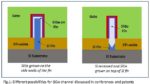
The next transition from current FinFET devices at advanced process nodes is the “nanosheet” device, as depicted in the figure below. [1]
The FinFET provides improved gate-to-channel electrostatic control compared to a planar device, where the gate traverses three sides of the fin. The “gate-all-around” characteristics… Read More
As I have discussed before, I believe that IEDM is the premier technical conference for understanding leading edge process technologies. Beginning this coming weekend, this year’s edition of IEDM will be held virtually, and I highly recommend attending.
The conference held a press briefing last Monday. The tutorial and short… Read More
With the announcement of early PDK availability for the 3nm GAA process node, designers are extremely interested in the characteristics of the new “gate-all-around” transistor structure and how it compares to the existing FinFET device. The GAA transistor has been denoted as a (horizontal) nanowire or nanosheet.
I will talk… Read More
We live in an age of abundant information. There is a tremendous exchange of ideas crisscrossing the world enabling new innovative type of products to pop up daily. Therefore, in this era there is a greater need to understand competitive intelligence. Corporate companies today are interested in what other competitors are brewing… Read More
At IEDM in December I had a chance to interview Thomas Ernst about the paper “Performance and Design Considerations for Gate-All-around Stacked-NanoWires FETs” by Leti and STMicroelectonics.
Leti published the first stacked nanowire in 2006, it was very new then, now stacked nanowire/nanosheets are starting… Read More