I attended the recent International Electron Devices Meeting (IEDM) last week. Many of the sessions are too technical and too far away from high volume manufacture to make good topics for a blog post. As a Fellow from IBM said about 5nm at and earlier IEDM, “none of these ideas will impact 5nm. It takes ten years for a solution to from and IEDM paper to HVM. So 5nm will be something like FinFET with some sort of copper interconnect.” And so it turned out to be.
Often there are late submissions that IEDM accepts, usually from important manufacturers such as Intel or TSMC giving the first details of their next generation process. Unfortunately, over the years, these papers have got less informative and rarely include key measures such as the pitches on the most critical layers.
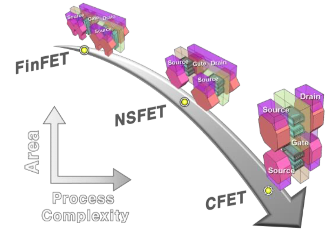
This year there was a late paper from TSMC titled Complementary Field-Effect Transistor (CFET) Demonstration at 48nm Gate Pitch for Future Logic Technology Scaling. A CFET is a CMOS process where the transistors are stacked vertically, rather than being in the same plane as with all previous logic processes: planar, FinFET, nanosheet field effect transistors (NSFET, also known as gate-all-around or GAA). The paper was by about 50 different authors that I’m not going to list, and was presented by Sandy Liao. She said it was “late news” since it is very recent work.
Presumably, TSMC will have a CFET process in the future, but this paper described early research on manufacturability. The process stacks the n-transistor on top of the p-transistor. In the Q&A Sandy was asked what motivated this decision. She said that it wasn’t cast in stone and could get changed in the future, but putting PMOS on the bottom makes handling strain easier. TSMC calls this monolithic CFET or mCFET.
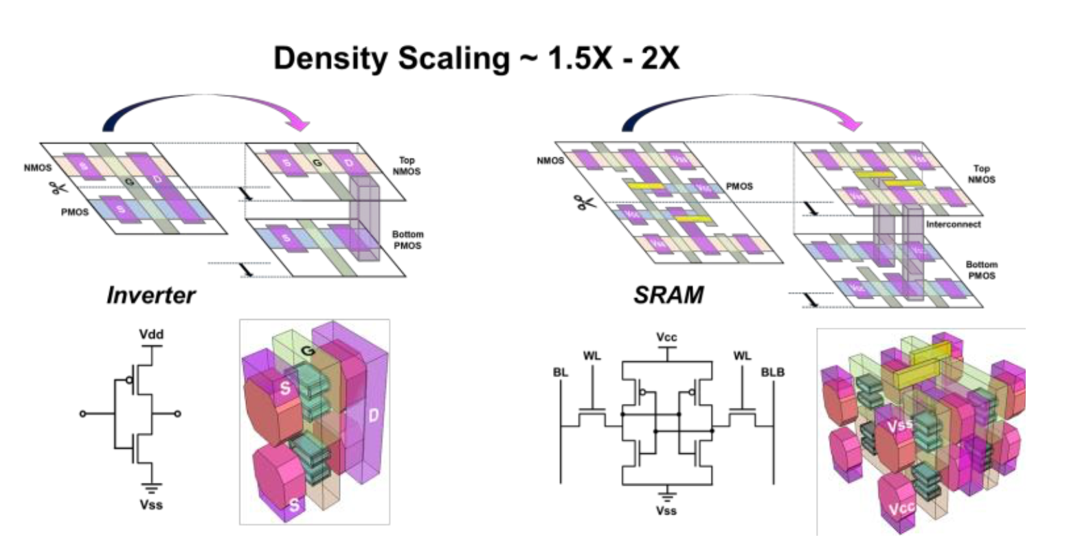
CFET can create an area reduction of 1.5X to 2X, he said. There still has to be space for some vertical routing so you don’t usually get the full 2X you might expect from stacking the transistors. Previous studies of CFET manufacturing have used relaxed gate pitches, and don’t succeed in getting gate pitches around 50nm. So this TSMC study is the first that uses a gate pitch of 48nm, which Sandy said is “pertinent to industry-level advanced node scaling.”
To accomplish this, there is a middle dielectric isolation, inner spacer, and n/p source-drain isolation. This process provides a robust foundation for future mCFET advancement which will require further innovation and additional architectural features.

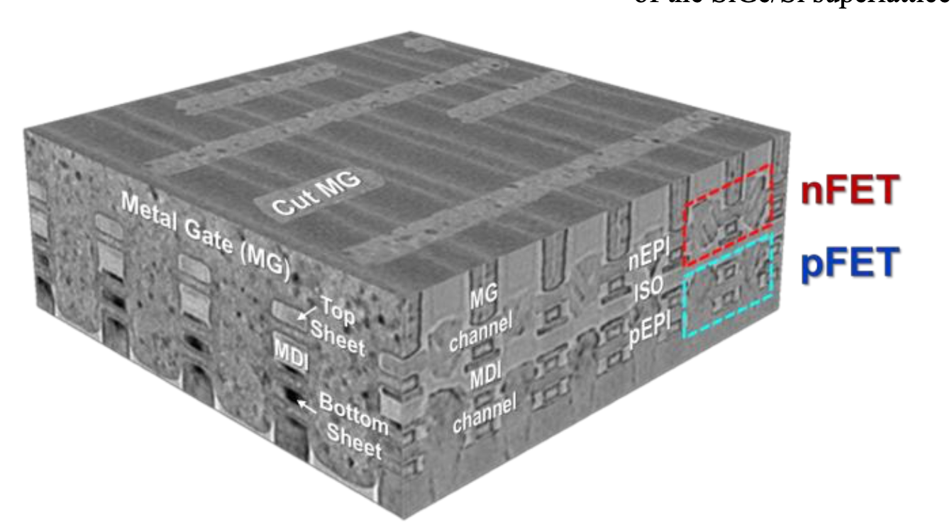
Here is a TEM demonstration of the mCFET. As I already said, the nFETs are on top and the pFETs on the bottom. Both types of transistors have the channel surrounded by a single metal gate.

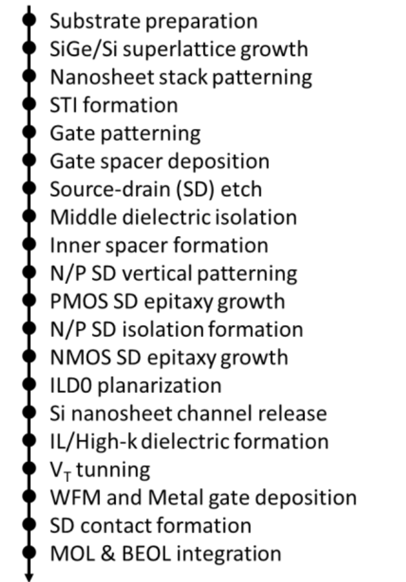
Sandy said she would provide some details of the fabrication process “but not too much”. It is a 20-step flow, although obviously there are many sub-steps inside each step. For now, the process is expensive to manufacture she said in time engineers will solve that and so the process will have value. Below are the 20 steps.

By introducing a middle dielectric isolation, inner spacer, and n/p source-drain isolation, the vertically stacked transistors have a survival rate of over 90% with high on-state current and low leakage. There is a six-orders-of magnitude Ion/Ioff current ratio.
Sandy’s conclusion:
- This is just the beginning, and there is a long way to go. But transistors in high volume cannot be worse than this. We need work hard to generate process features real yielding circuits with better characteristics.
- This is just a study to pave the way for a practical process architecture that can fuel future logic technology, scaling, and PPAC advancement.
Also Read:
Analog Bits Leads the Way at TSMC OIP with High-Accuracy Sensors
TSMC N3E is ready for designs, thanks to IP from Synopsys
The True Power of the TSMC Ecosystem!
Share this post via:


Comments
One Reply to “IEDM: TSMC Ongoing Research on a CFET Process”
You must register or log in to view/post comments.