

At its 2026 Technology Symposium, TSMC delivered a clear message: the AI era has entered a new phase. The primary constraint is no longer model capability, but the systems required to run those models at scale. Addressing this shift will demand significant advances in semiconductor technology, spanning compute, memory, interconnects, and power efficiency.
From Model Scaling to System Scaling
Over the past several years, AI progress was largely driven by scaling models. In other words, expanding parameter counts, improving training methods, and unlocking new reasoning capabilities. That paradigm is now evolving. In 2026, the bottleneck has shifted to system-level challenges such as compute throughput, memory bandwidth, interconnect efficiency, power delivery, and deployment scale. AI is becoming fundamentally a systems problem rather than a purely algorithmic one.
This transition is especially visible in the rise of enterprise AI agents. These systems are moving beyond narrow task assistance to orchestrating workflows, integrating enterprise data, and enabling more autonomous decision-making. As a result, they require high reliability, strong security, and sustained performance, all of which significantly increase infrastructure demands.
Explosive Growth in AI Compute Demand
AI compute demand continues to grow at an extraordinary pace, driven by both training and inference. On the training side, large language models have already driven roughly fivefold annual increases in compute requirements. And the shift toward multimodal AI which combines text, vision, audio, and real-world signals, is accelerating this trend further. Training demand alone is expected to increase by another order of magnitude.
Even more striking is the growth in inference. Token generation has increased more than 500 times between 2022 and 2025, and new techniques such as chain-of-thought reasoning are significantly increasing compute per query. The emergence of agent-based AI systems could multiply this demand again, while large-scale multimodal deployments may push total inference workloads toward million-fold growth. As a result, inference is rapidly becoming the dominant driver of compute infrastructure expansion.
AI Is Expanding Beyond the Cloud
AI is no longer confined to centralized cloud environments; it is rapidly expanding into edge and physical domains. At the edge, inference is increasingly being performed directly on devices such as PCs, smartphones, and wearables. This shift enables lower latency, improved privacy, and real-time responsiveness, and is driving the widespread adoption of dedicated AI accelerators like NPUs in consumer hardware.
At the same time, physical AI is bringing intelligence into the real world through robotics and embodied systems. These applications require tight integration of AI with sensing, actuation, and real-time control, all within strict power and reliability constraints. Together, these trends highlight the growing need for silicon solutions that can balance performance, efficiency, and compact form factors across a wide range of environments.
Data Center Scaling Enters Hyper-Growth
The rapid expansion of AI workloads is fundamentally reshaping data center infrastructure. Annual capacity additions, which previously grew at a steady rate of around 5 to 6 gigawatts, are now expected to reach 30 to 40 gigawatts per year. At the same time, overall data center investment growth has accelerated from roughly 10 percent annually before the rise of generative AI to more than 30 percent per year through the end of the decade.
This growth is not just about adding capacity; it is about delivering efficient, reliable, and scalable systems. Energy efficiency and total cost of ownership are becoming central concerns, making semiconductor-level improvements critical to the sustainability of AI infrastructure.
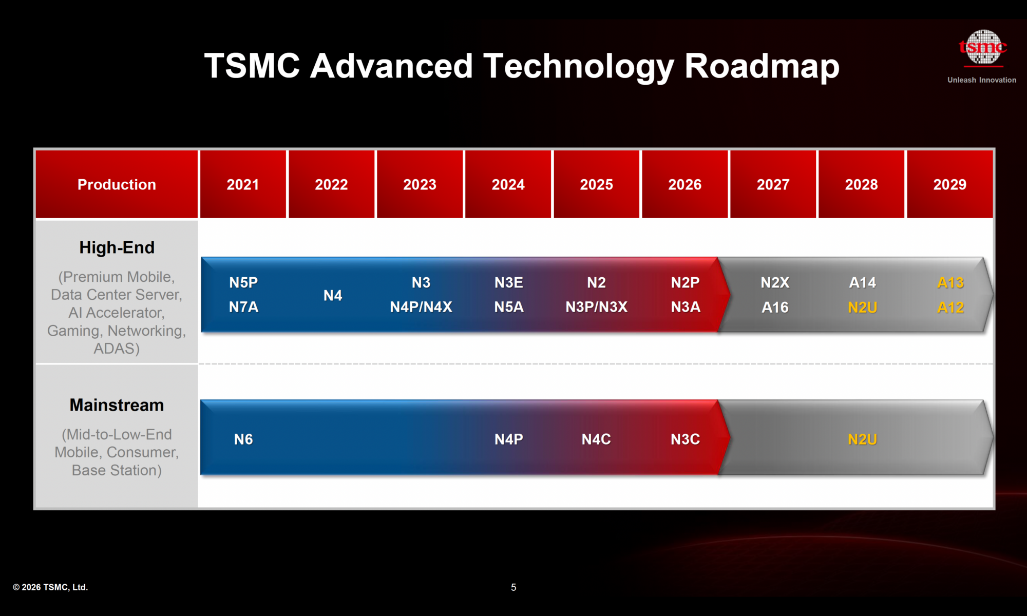
TSMC’s Technology Roadmap: Key Innovations
A14: Next-Generation Logic Platform (2028)
A14 represents TSMC’s next major step in logic technology, combining second-generation nanosheet transistors with NanoFlex Pro architecture and continued backend scaling innovations. Compared with the N2 node, A14 is expected to deliver a 10 to 15 percent speed improvement at the same power or a 25 to 30 percent power reduction at the same speed, along with approximately 1.2 times the logic density.
A central innovation in A14 is NanoFlex Pro, which enhances standard cell architecture to improve area efficiency and performance per watt. This is complemented by significant backend scaling advancements, including tighter metal pitch and reduced minimum metal area, enabling higher transistor density and improved overall efficiency. Together, these innovations demonstrate that progress at advanced nodes now depends on full-stack optimization rather than transistor scaling alone.
A13 and A12: Extending the Platform
Building on A14, TSMC is extending its roadmap with A13 and A12 technologies, both targeted for production around 2029. A13 further improves density and efficiency while maintaining backward compatibility with A14, enabling smoother design migration for customers. A12 introduces backside power delivery, a major innovation that improves power integrity and performance by separating power and signal routing. These developments reflect a broader shift toward holistic scaling, where power delivery and system-level considerations play an increasingly important role.
N2 Family: Nanosheet Era in Production
The N2 node marks TSMC’s transition from FinFET to nanosheet transistor architecture, delivering improved electrostatic control, reduced leakage, and lower operating voltage. These benefits translate into tangible efficiency gains in real-world applications.

The N2 family includes several variants designed to address different performance needs. The base N2 node entered production in 2025, followed by N2P in 2026 as an enhanced version. N2X, expected in 2027, targets high-performance applications with additional frequency gains, while N2U, planned for 2028, integrates NanoFlex Pro enhancements to further improve performance and power efficiency. This expanding family underscores the importance of offering flexible solutions tailored to diverse workloads.
Advanced Packaging and 3D Integration
As AI workloads continue to scale, advanced packaging technologies are becoming as critical as process nodes themselves. TSMC is advancing its chiplet and 3D integration capabilities with improvements such as second-generation CoWoS technology, which reduces interconnect resistance and enables higher bandwidth through finer I/O pitch.
These innovations allow for denser integration of compute and memory, improving performance and energy efficiency at the system level. In the AI era, packaging is no longer a secondary consideration but a key enabler of overall system performance.
N3: Today’s Workhorse Node
While future nodes attract significant attention, the N3 family remains the backbone of current high-performance computing. It is widely deployed across mobile devices, CPUs, AI accelerators, and networking applications, with multiple variants such as N3P and N3C supporting different use cases. Strong customer adoption and a robust pipeline of new designs highlight the continued importance of mature leading-edge nodes in delivering value across the ecosystem.
Summary
TSMC’s roadmap reflects a fundamental shift in the semiconductor industry. As AI continues to scale, the primary challenge is no longer developing more powerful models, but building the infrastructure required to support them efficiently. This requires innovation across the entire technology stack, from transistors and interconnects to packaging and system architecture.
In this new era, success will depend on the ability to deliver not just better chips, but better systems. The companies that can integrate performance, efficiency, and scalability at every level of the stack will define the future of AI—and increasingly, that future is being shaped at the silicon level.
Also Read:
TSMC Technology Symposium 2026 Overview
TSMC to Elon Musk: There are no Shortcuts in Building Fabs!
TSMC Technology Symposium 2026: Advancing the Future of Semiconductor Innovation
Share this post via:


Comments
There are no comments yet.
You must register or log in to view/post comments.