
")
Dr. Y.J. Mii joined TSMC in 1994 as a manager at Fab 3 before moving into the company’s research and development organization in 2001. He was appointed Vice President of R&D in 2011 and later advanced to Senior Vice President in November 2016.
Over more than 20 years at TSMC, Dr. Mii has played a central role in advancing and manufacturing cutting-edge CMOS technologies across both fab operations and R&D. He led the successful development of key process nodes, including 90nm, 40nm, and 28nm. In addition, he has driven innovation in more advanced technologies—such as 16nm, 7nm, 5nm, and 3nm—helping sustain TSMC’s leadership position in the global semiconductor foundry industry.
In recognition of his leadership in research and development, Dr. Mii received the IEEE Frederik Philips Award in 2022. Prior to joining TSMC, he worked as a research staff member at the IBM Research Center.
Dr. Mii holds 34 patents worldwide, including 25 granted in the United States. He earned his bachelor’s degree in electrical engineering from National Taiwan University, and both his master’s and Ph.D. in electrical engineering from University of California, Los Angeles.
Dr. Y.J. Mii’s presentation outlines the company’s continued leadership in semiconductor technology and its roadmap for future innovation across advanced logic, system integration, and specialty platforms. The talk emphasizes TSMC’s commitment to delivering cutting-edge technologies that support next-generation applications such as AI, high-performance computing (HPC), and mobile devices.

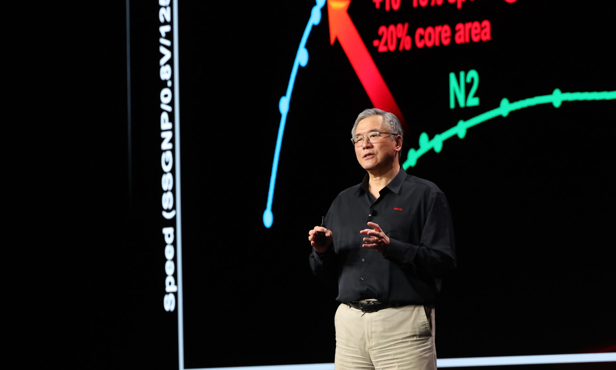
TSMC is introducing several new advanced nodes, including A14, A13, and A12, which extend its leadership into what is described as the “Armstrong era.” The A14 node represents a second-generation nanosheet transistor technology and incorporates NanoFlex Pro, achieving significant improvements in performance, power, and area (PPA). Compared to the 2nm (N2) node, A14 delivers 10–15% speed improvement or 25–30% power reduction, along with notable density gains. Production is expected by 2028. Building on this, A13 offers further optimization, including a 6% die size reduction through optical shrink and improved efficiency, while maintaining backward compatibility with A14 designs.
TSMC’s 2nm family is also expanding, including N2, N2P, N2X, and N2U. These technologies are already seeing strong customer adoption, particularly driven by AI and HPC demands. N2 entered production recently, with N2P and A16 progressing toward volume production. The N2U variant further enhances performance and efficiency while maintaining compatibility with N2P, offering incremental speed and power improvements. The rapid increase in customer tapeouts highlights the strong industry demand for these advanced nodes.

Beyond nanosheet transistors, TSMC is investing in future innovations such as complementary field-effect transistors (CFET), which stack nFET and pFET vertically to enable continued scaling. The company has already demonstrated early CFET implementations and advanced SRAM designs with reduced footprint. Additionally, research into two-dimensional materials shows significant improvements in transistor performance, suggesting further opportunities for scaling and energy efficiency.
Interconnect technology is another key focus area. TSMC is improving copper-based interconnects by reducing resistance and capacitance through new materials and structures. It is also exploring alternative materials and air-gap techniques to further enhance performance. Long-term research includes novel 2D conductors that could dramatically reduce contact resistance compared to existing solutions.
In system integration, TSMC is advancing its HPC platform through technologies such as CoWoS, SoIC, and SoW. CoWoS remains a central platform for scaling, with increasing reticle sizes and high-bandwidth memory (HBM) integration planned through 2030. SoW technology aims to integrate entire systems on a wafer, enabling massive computing capabilities for AI workloads. Meanwhile, SoIC 3D stacking continues to evolve, improving interconnect density and power efficiency.

The company is also developing photonic integration technologies like the Compact Universal Photonic Engine (COUPE), which enables high-speed, low-power optical data transmission. These solutions significantly outperform traditional copper interconnects in both power efficiency and latency, and future advancements aim to further increase bandwidth and scalability.

In the specialty technology segment, TSMC highlights advancements in automotive, RF, memory, and display technologies. The N3A node is now fully automotive-qualified, while future nodes like N2A are in development. RF technologies such as N4C RF deliver improved power efficiency and performance for edge AI applications. In memory, embedded flash is being replaced by alternatives like resistive RAM (RRAM) and MRAM, which offer better scalability and performance. Display innovations, including high-voltage platforms, enable more efficient and compact designs for smartphones and smart glasses.
Bottom line: TSMC’s roadmap demonstrates a comprehensive approach to semiconductor innovation, spanning advanced nodes, new transistor architectures, system integration, and specialized technologies. The company aims to empower customers with industry-leading solutions that drive future computing advancements and enable emerging applications across multiple industries.
Also Read:
Enabling Next-Generation AI Through Advanced Packaging and 3D Fabric Integration
Dr. Cliff Hou and the TSMC N2 Process Technology
The Shift to System-Level AI Drives Next-Generation Silicon
TSMC Technology Symposium 2026 Overview
Share this post via:


Comments
There are no comments yet.
You must register or log in to view/post comments.