You are currently viewing SemiWiki as a guest which gives you limited access to the site. To view blog comments and experience other SemiWiki features you must be a registered member. Registration is fast, simple, and absolutely free so please,
join our community today!
Dr. Y.J. Mii joined TSMC in 1994 as a manager at Fab 3 before moving into the company’s research and development organization in 2001. He was appointed Vice President of R&D in 2011 and later advanced to Senior Vice President in November 2016.
Over more than 20 years at TSMC, Dr. Mii has played a central role in advancing and manufacturing… Read More
Even though this is the 16th OIP event please remember that TSMC has been working closely with EDA and IP companies for 20+ years with reference flows and other design enablement and silicon verification activities. The father of OIP officially is Dr. Morris Chang who named it the Grand Alliance. However, Dr. Cliff Hou is the one … Read More
For many years, monolithic chips defined semiconductor innovation. New microprocessors defined new markets, as did new graphics processors, and cell-phone chips. Getting to the next node was the goal, and when the foundry shipped a working part victory was declared. As we know, this is changing. Semiconductor innovation is… Read More
Last week TSMC announced the opening of an advanced backend fab for the expansion of the TSMC 3DFabric System Integration Technology. It’s a significant announcement as the chip packaging arms race with Intel and Samsung is heating up.
Fab 6 is TSMC’s first all-in-one advanced packaging and testing fab which is part of the… Read More
The TSMC Open Innovation Platform (OIP) event brings together a wide array of companies reporting cutting edge work that are part of TSMC’s rather substantial ecosystem. The event covers everything from high-performance computing to mobile, automotive, IoT, RF and 3D IC design. Of particular interest for this post is a presentation… Read More
The recent TSMC Technology Symposium provided several announcements relative to their advanced packaging offerings.
General
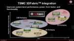
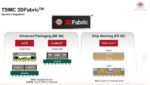
3DFabricTM
Last year, TSMC merged their 2.5D and 3D package offerings into a single, encompassing brand – 3DFabric.
2.5D package technology – CoWoS
The 2.5D packaging options are divided into the CoWoS… Read More
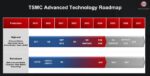
Here are the Top 10 highlights from the recent TSMC 2018 Technology Symposium, held in Santa Clara CA. A couple of years ago, TSMC acknowledged the unique requirements of 4 different market segments, which has since guided their process development strategy — Mobile, High-Performance Computing (HPC), Automotive, and… Read More
Years ago my good friend Herb Reiter promoted the importance of 2.5D packaging to anybody and everybody who would listen including myself. Today Herb’s vision is in production and the topic of many papers, webinars, and conferences. According to Herb, and I agree completely, advanced IC packaging is an important technology for… Read More
Open Silicon hosted a webinar today focusing on their High Bandwidth Memory (HBM) IP-subsystem product offering. Their IP-subsystem is based on the HBM2 standard and includes blocks for the memory controller, PHY and high-speed I/Os, all targeted to TSMC 16nm FF+ process. The IP-subsystem supports the full HBM2 standard with… Read More
When someone says, “2.5D packaging” my first thought is TSMC and my second thought is Herb Reiter. Herb has more than 40 years of semiconductor experience and he has been a tireless promoter of 2.5D packaging for many years. Herb writes for and works with industry organizations on 2.5D work groups and events at conferences… Read More