
")
L.C. leads efforts in design enablement, ensuring that the company can meet the diverse and evolving requirements of its global customer base. Prior to this, he headed the Design and Technology Platform organization starting in 2018.
Since joining TSMC in 2000, Dr. Lu has held multiple leadership positions in design services. He has worked closely with process R&D teams to pioneer Design and Technology Co-Optimization (DTCO), improving speed, power efficiency, and density in advanced process technologies. He has also collaborated extensively with ecosystem partners through the TSMC Open Innovation Platform (OIP), helping deliver comprehensive design solutions and intellectual property for a wide range of applications, including high-performance computing, automotive, RF, and advanced 2.5D and 3D designs.
Dr. Lu’s contributions have earned him significant recognition. He received Taiwan’s National Outstanding Manager Award in 2012 and was named a TSMC Senior Fellow in 2025. He is also one of the company’s most prolific inventors, holding more than 100 patents worldwide.
He earned his bachelor’s degree in electrical engineering from National Taiwan University, a master’s degree in computer science from National Tsing Hua University, and a Ph.D. in computer science from Yale University.
L.C.’s presentation focuses on advanced design-technology co-optimization (DTCO), packaging innovations, and AI-driven methodologies that enable continued scaling in performance, power, and area (PPA) for next-generation semiconductor systems. The discussion highlights how tightly coupled design and process innovations, along with system-level integration, are critical to sustaining Moore’s Law in the era of AI and HPC.
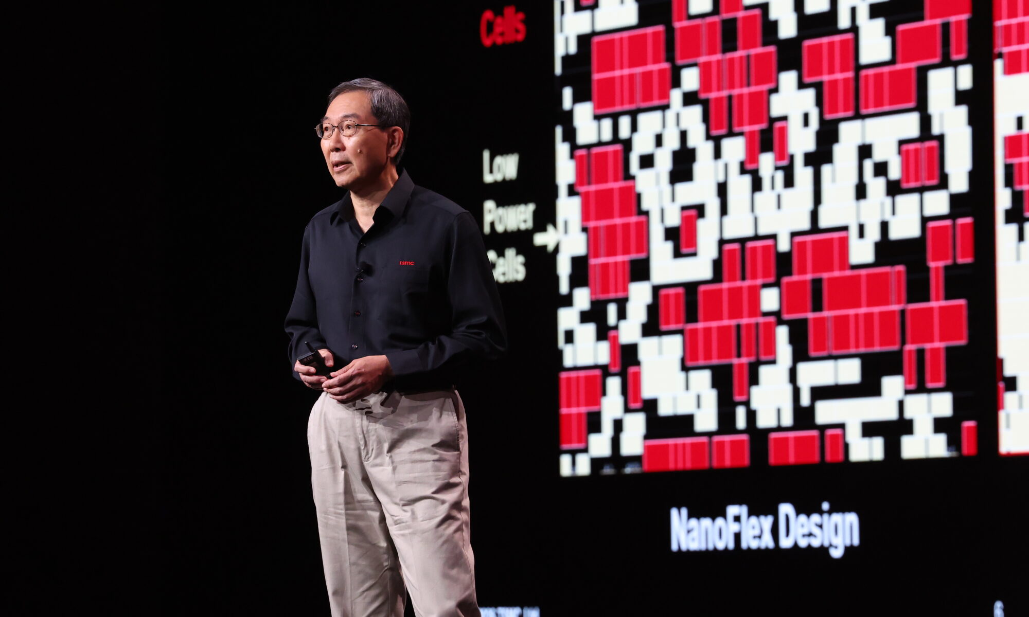
At the device and design level, TSMC emphasizes DTCO and design-driven cell (DDCL) innovations to achieve node-to-node scaling from N5 through N2 and into A14. The introduction of NanoFlex and NanoFlex Pro architectures enables flexible standard cell design with significant gains in efficiency. N2 NanoFlex achieves up to 50% speed improvement at constant voltage or 50% power reduction at constant performance compared to traditional cells. Building on this, A14 NanoFlex Pro introduces a 1.5× cell height merged oxide diffusion (OD) architecture, significantly improving OD utilization and enabling tighter placement of high-speed and low-power cells. This results in 10–15% speed gains and ~20% area reduction relative to N2, effectively delivering multi-node scaling benefits within a single generation.

Further enhancements in N2P and N2U nodes incorporate advanced DTCO and power delivery optimizations. Hybrid dual-rail architectures reduce minimum operating voltage (Vmin) by over 200 mV compared to single-rail designs, achieving approximately 40% energy savings. N2U extends N2P with incremental improvements—3–4% higher performance or 8–10% lower power—while maintaining full compatibility with existing design rules and IP, ensuring smooth adoption for customers.
EDA readiness and AI integration are key enablers of these advanced nodes. TSMC collaborates closely with electronic design automation (EDA) partners to ensure tool readiness and to incorporate AI-enhanced workflows. Agentic AI systems are being deployed across design cycles to optimize block placement, routing, and performance, improving both productivity and design quality. These AI techniques are also applied to analog and RF design, enabling efficient migration across process nodes and accelerating time-to-market.
At the system level, TSMC’s advanced packaging technologies—particularly CoWoS, SoIC, and 3D Fabric—play a central role in enabling AI scaling. CoWoS technology continues to scale reticle size and integration capacity, allowing significant increases in compute density. From 2024 to 2029, the number of transistors in a single CoWoS system is projected to increase by 48×, driven by larger package sizes, increased system-on-chip (SoC) counts, and transition to advanced nodes such as TSMC A14.

Memory bandwidth scaling is similarly aggressive, with high-bandwidth memory (HBM) integration increasing both capacity and throughput. HBM stacks are expected to grow from 8 to 24, while I/O bandwidth per stack doubles and data rates increase significantly, resulting in an overall 34× bandwidth improvement. This scaling is supported by advancements in both DRAM technology and logic-based base dies fabricated on advanced nodes.
Interconnect performance is improved through finer pitch scaling in both 2.5D and 3D integration. In CoWoS, micro-bump pitch reduction enhances bandwidth density and energy efficiency, while in SoIC, scaling to ~4.5 µm bump pitch delivers up to 4× bandwidth density and substantial energy savings. Additionally, silicon photonics integration via CUPE optical engines provides high-speed, low-latency interconnects, achieving 5–10× power efficiency improvements and 10–20× latency reduction compared to traditional electrical links.
Power delivery and thermal management are identified as critical challenges in AI systems due to increasing compute density. TSMC addresses these through advanced capacitance solutions such as metal-insulator-metal (MIM) capacitors and embedded deep trench capacitors (eDDC), achieving over 10× improvements in capacitance density and reducing voltage droop significantly. Thermal optimization techniques—including improved packaging materials, hotspot spreading, and structural enhancements—reduce thermal resistance by up to 40%, ensuring reliable operation under high power conditions.
Bottom line: TSMC is advancing design methodologies through 3D IC design standardization and AI-driven automation. The introduction of “3D Blocks” as a modular design language aims to streamline 3D IC workflows and enhance collaboration across the ecosystem, with ongoing efforts toward IEEE standardization. Combined with generative AI and agent-based design optimization, these innovations promise substantial improvements in productivity and scalability for complex chip-package co-design.
Also Read:
Dr. Cliff Hou and the TSMC N2 Process Technology
TSMC Technology Symposium 2026 Overview
Share this post via:


Comments
There are no comments yet.
You must register or log in to view/post comments.