You are currently viewing SemiWiki as a guest which gives you limited access to the site. To view blog comments and experience other SemiWiki features you must be a registered member. Registration is fast, simple, and absolutely free so please,
join our community today!
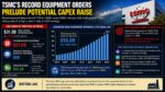
TSMC’s latest Board of Directors capital appropriation announcement may appear mixed on the surface, but a closer look reveals one important conclusion: The company is quietly setting the stage for another potential upward revision to its already aggressive 2026 capital expenditure outlook. The headline figure of $31.3B … Read More
L.C. leads efforts in design enablement, ensuring that the company can meet the diverse and evolving requirements of its global customer base. Prior to this, he headed the Design and Technology Platform organization starting in 2018.
Since joining TSMC in 2000, Dr. Lu has held multiple leadership positions in design services.… Read More
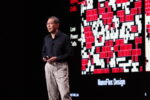
Yes, it is that time of year again, the 2026 TSMC Technology Symposium kick-off event in Silicon Valley. TSMC has never been in a better position to forecast the future of semiconductor technology and the industry itself. TSMC closely collaborates with the top semiconductor companies around the world and the top players in the … Read More
The main program for the 70th IEDM opened on Monday morning in San Francisco with an excellent keynote from Dr. Yuh-Jier Mii, Executive Vice President and Co-Chief Operating Officer at TSMC. Dr. Mii joined TSMC in 1994. Since then, he has contributed to the development and manufacturing of advanced CMOS technologies in both fab
…
Read More
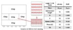
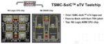
At the recent TSMC OIP Ecosystem Forum in Santa Clara, there was an important presentation that laid the groundwork for a great deal of future innovation. Alchip and its IP and EDA partner Synopsys presented Efficient 3D Chiplet Stacking Using TSMC SoIC. The concept of 3D, chiplet-based design certainly isn’t new. SemiWiki maintains… Read More
Synopsys made significant announcements during the recent TSMC OIP Ecosystem Forum, showcasing a range of cutting-edge solutions designed to address the growing complexities in semiconductor design. With a strong emphasis on enabling next-generation chip architectures, Synopsys introduced both new technologies and … Read More
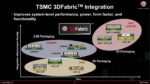
Last week TSMC announced the opening of an advanced backend fab for the expansion of the TSMC 3DFabric System Integration Technology. It’s a significant announcement as the chip packaging arms race with Intel and Samsung is heating up.
Fab 6 is TSMC’s first all-in-one advanced packaging and testing fab which is part of the… Read More
Advanced 2.5D/3D Packaging Roadmapby Tom Dillinger on 01-03-2022 at 6:00 amCategories: Events, Semiconductor, TSMC
Frequent SemiWiki readers are no doubt familiar with the advances in packaging technology introduced over the past decade. At the recent International Electron Devices Meeting (IEDM) in San Francisco, TSMC gave an insightful presentation sharing their vision for packaging roadmap goals and challenges, to address the growing… Read More
TSMC recently held their 10th annual Open Innovation Platform (OIP) Ecosystem Forum. An earlier article summarized the highlights of the keynote presentation from L.C. Lu, TSMC Fellow and Vice-President, Design and Technology Platform, entitled “TSMC and Its Ecosystem for Innovation” (link).
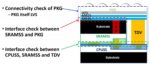
Overview of 3D Fabric
The TSMC… Read More
Design Considerations for 3DICsby Tom Dillinger on 12-14-2020 at 6:00 amCategories: Events, Semiconductor, TSMC
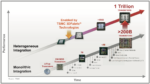
The introduction of heterogeneous 3DIC packaging technology offers the opportunity for significant increases in circuit density and performance, with corresponding reductions in package footprint. Yet, the implementation of a complex 3DIC product requires a considerable investment in methodology development for all… Read More