The 15th TSMC Open Innovation Platform® (OIP) was held last week. In preparation we did a podcast with one of the original members of the TSMC OIP team Dan Kochpatcharin. Dan and I talked about the early days before OIP when we did reference flows together. Around 20 years ago I did a career pivot and focused on Strategic Foundry Relationships. The importance of the foundries was clear to me and I wanted to be an integral part of that ecosystem. As it turns out it was a great career move, absolutely.

Before I get to the importance of the early TSMC reference flow days let’s talk about the recent OIP event. It was held at the Santa Clara Convention Center and it was a full house. For those other semiconductor event coordinators, if you want full semiconductor attendance use the Santa Clara Convention Center. Local hotels or the San Jose Convention Center are not convenient and convenience means attendance. TSMC switched to the Santa Clara Convention Center from San Jose a few years back and the rest as they say is history, TSMC hosts the best semiconductor networking events.
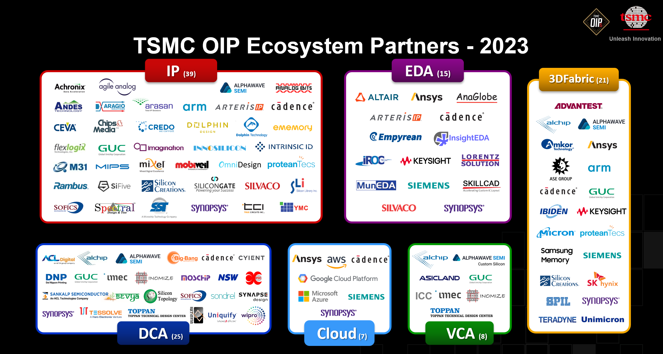
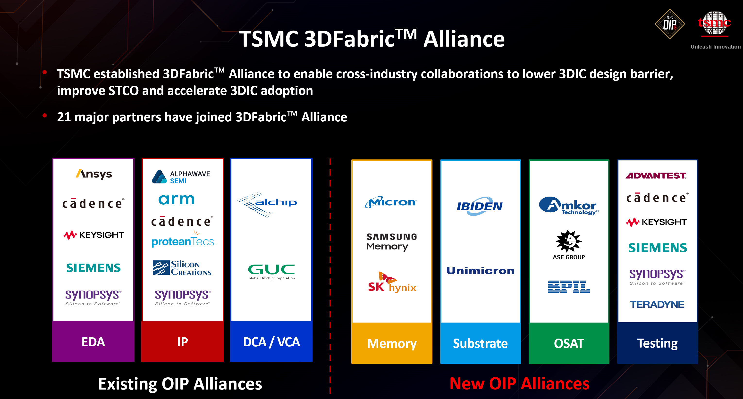
This year OIP was all about packaging and rightly so. It is the next foundry battleground and TSMC is once again building a massive ecosystem appropriately named the 3D Fabric Alliance:

TSMC Announces Breakthrough Set to Redefine the Future of 3D IC New 3Dblox 2.0 and 3DFabric Alliance Achievements Detailed at 2023 OIP Ecosystem Forum
“As the industry shifted toward embracing 3D IC and system-level innovation, the need for industry-wide collaboration has become even more essential than it was when we launched OIP 15 years ago,” said Dr. L.C. Lu, TSMC fellow and vice president of Design and Technology Platform. “As our sustained collaboration with OIP ecosystem partners continues to flourish, we’re enabling customers to harness TSMC’s leading process and 3DFabric technologies to reach an entirely new level of performance and power efficiency for the next-generation artificial intelligence (AI), high-performance computing (HPC), and mobile applications.”
L.C. Lu has been part of the TSMC OIP since the beginning, he worked for Dr. Cliff Hou. From 1997 to 2007 Cliff established the TSMC PDK and reference flow development organizations which then led to the OIP. Cliff Hou is now TSMC Senior Vice President, Europe & Asia Sales and Research & Development / Corporate Research.
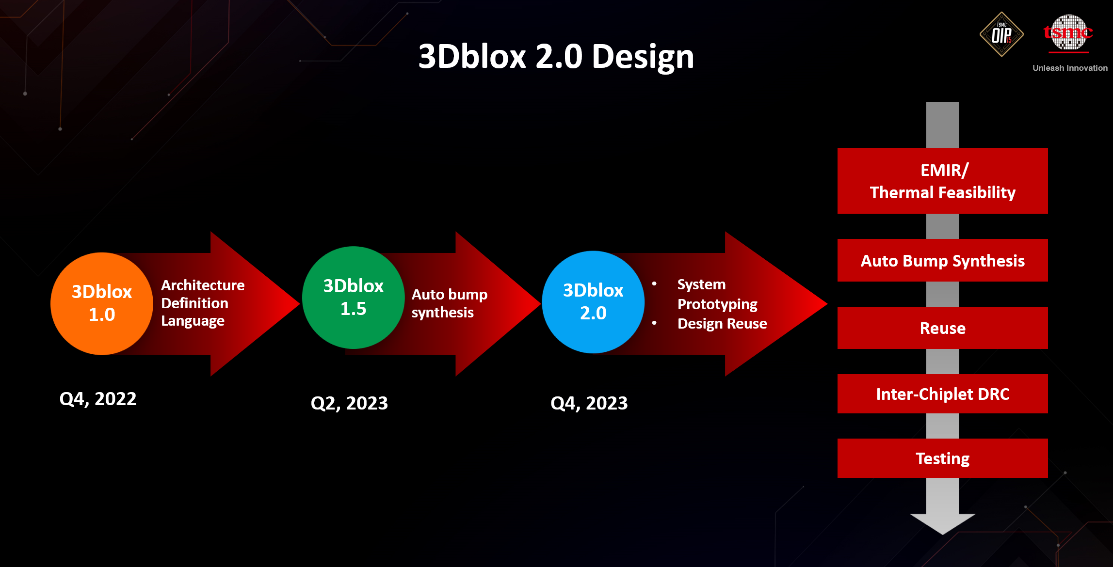
L.C. updated us on the progress of the 3D Alliance and 3D Blox which is an incredible piece of technology that is open to all customers, partners and competitors alike. It is an industry standard in the making for sure. We covered 3D Blox HERE and TSMC gave us this update:
Introduced last year, the 3Dblox open standard aims to modularize and streamline 3D IC design solutions for the semiconductor industry. With contribution from the largest ecosystem of companies, 3Dblox has emerged as a critical design enabler of future 3D IC advancement.
The new 3Dblox 2.0, launched today, enables 3D architecture exploration with an innovative early design solution for power and thermal feasibility studies. The designer can now, for the first time in the industry, put together power domain specifications and 3D physical constructs in a holistic environment and simulate power and thermal for the whole 3D system. 3Dblox 2.0 also supports chiplet design reuse features such as chiplet mirroring to further improve design productivity.
3Dblox 2.0 has won support from key EDA partners to develop design solutions that fully support all TSMC 3DFabric offerings. Those comprehensive design solutions provide designers with key insights to make early design decisions, accelerating design turnaround time from architecture to final implementation.
TSMC also launched the 3Dblox Committee, organized as an independent standard group, with the goal to create an industry-wide specification that enables system design with chiplets from any vendors. Working with key members including Ansys, Cadence, Siemens, and Synopsys, the committee has ten technical groups of different subjects and proposes enhancements to the specs and maintain the interoperability of EDA tools. Designers can now download the latest 3Dblox specifications from the 3dblox.org website and find more information about 3Dblox and its tool implementation by EDA partners.

Back to the reference flows, I was the Strategic Foundry Relationship Advisor for Solido Design Automation out of Saskatoon Canada and Berkeley Design Automation (BDA) in Silicon Valley at the time. Back then EDA included a lot of point tools inside the design flow since no one company could do it all. So all of the point tool companies looked to TSMC for guidance on how to interoperate inside a customer’s design flow. This was not only valuable experience, it provided much needed exposure for EDA start-ups to the TSMC customer base. In the case of Solido and BDA, it not only led to rapid adoption by TSMC’s top customers, TSMC itself licensed the tools for internal use which is the ultimate seal of approval. Solido and BDA were both acquired by Seimens EDA and their close relationships with TSMC was a big part of that transaction, believe it.
A similar process was developed for silicon proven IP. I am also a Foundry Relationships Advisor for IP companies and not only do we get access to TSMC’s top customers, TSMC allows access to PDKs and taught us how to silicon prove our products. Notice on the TSMC OIP partner list the biggest market segment is IP companies for these exact reasons. IP is a critical enabler for the foundry business and getting silicon right the first time is what OIP is all about.
Bottom line: In the foundry business it’s all about collaboration and TSMC built this massive ecosystem from the ground up. Not only does it reduce customer risk of designing to new processes, the close collaboration between TSMC and the ecosystem partners multiplies the total annual ecosystem R&D investments exponentially.
Also Read:
The TSMC Pivot that Changed the Semiconductor Industry!
Share this post via:


Comments
There are no comments yet.
You must register or log in to view/post comments.