TSMC originally brought the pure-play foundry business to the United States in 1996 through a joint venture with customers Altera, Analog Devices, ISSI, and private investors (no government money). Altera is now part of Intel but ADI is still a top TSMC customer and enthusiastic supporter. I have seen the ADI CEO Vincent Roche present at recent TSMC events and his TSMC partnership story is compelling. This joint venture was part of TSMC’s customer centric approach to business, responding directly to customer requests.
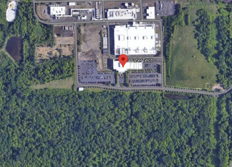
The WaferTech fab was established in Camas Washington (just North of the Oregon/Washington border) in 1996 with an investment of more than $1B which was a huge amount of money at the time. Production started two years later at .35 micron which was part of the Philips technology transfer that TSMC was founded upon. In 2000 TSMC bought out the partners and private investors, taking full control of the Washington fab. It is now called TSMC Fab 11 but clearly this fab was ahead of its time, absolutely.
From TSMC:
WaferTech focuses on Embedded Flash process technology while supporting a broad TSMC technology portfolio on line-widths ranging from 0.35-microns down to 0.16-microns. We specialize in helping companies deliver differentiated products and work with them on a number of customized and manufacturing “phase-in” projects. As a result, WaferTech delivers the latest generation semiconductors around the globe, supporting innovations in automotive, communications, computing, consumer, industrial, medical and military/aerospace applications.
To complement our world class process manufacturing services, WaferTech also provides test and analysis services at our Camas, Washington facility. Moreover, TSMC provides design, mask and a broad array of packaging and backend services at its other locations around the world. WaferTech also is a host for TSMC’s foundry-leading CyberShuttle™ prototyping services that help reduce overall design risks and production costs.
WaferTech, First U.S. Pure-play Foundry Ships Production Qualified Product ahead of Plan Issued by: Taiwan Semiconductor Manufacturing Company Ltd. Issued on: 1998/07/07
“With WaferTech on-line and shipping, TSMC customers gain another assured source for wafers produced to our standards of excellence,” said Ron Norris, president of TSMC, USA and a director of WaferTech. “Now TSMC is the only foundry in the world to transparently support customers from geographically dispersed sites.”
Ron Norris is another hire TSMC made with TI roots. Ron himself was a semiconductor legend. He started his career at TI and held executive level positions at Microchip in Arizona, Fairchild Semiconductor in Silicon Valley, and Data I/O Systems in Redmond WA, so he certainly knew the challenges of semiconductor manufacturing in the United States.
Historically, TSMC doesn’t just build fabs, TSMC builds communities. In fact, a TSMC fab itself is a community with everything you need to help maintain a work life balance. I have spent a lot of time in different fabs around the world but for the most part they were TSMC fabs in Taiwan. I still consider the Hsinchu Hotel Royal (walking distance from TSMC Fab 12A) as my second home. I remember flying in on my birthday one year and the staff had a mini birthday celebration when I arrived. Yes, they are that good, but I digress.
One thing you have to remember is that in Taiwan, working for TSMC brings status. You are a rockstar. Working for Samsung in South Korea has a similar aura. When TSMC breaks ground on a new fab location in Taiwan you can expect a whole support ecosystem to develop around it with everything a TSMC fab needs to be successful including housing and university level education for recruiting and employee growth.
Bottom line: Working for TSMC in Taiwan is like joining a very large and very successful family business.
Unfortunately, in Camas Washington, that was not the case. The WaferTech campus is a 23 acre complex housed on 260 acres. The main fabrication facility consists of a 130,000 square foot 200mm wafer fabrication plant. Additional fabs were planned but never built, a support ecosystem never formed, thus the TSMC Taiwan fab recipe was called out as a failure in the US.
Many reasons have been sited for this “failure” including high costs, problems attracting local talent, and timing (soft economy), but in my opinion it also had a lot to do with the rockstar factor. In the US we had forgotten or did not know yet how important semiconductors were to modern life and TSMC was not a big name in the US like it is today.
Now that TSMC is building fabs in Arizona, Kumamoto Japan, and Dresden Germany it will be interesting to see how different the TSMC experience is in these world wide locations.
Also Read:
How Taiwan Saved the Semiconductor Industry
Morris Chang’s Journey to Taiwan and TSMC
The First TSMC CEO James E. Dykes
Former TSMC President Don Brooks
The TSMC Pivot that Changed the Semiconductor Industry!
Share this post via:


Comments
5 Replies to “TSMC’s First US Fab”
You must register or log in to view/post comments.