The semiconductor industry’s incredible juggernaut has been powered by device innovations at its very core. Moreover, present-day enterprises encounter immense competitive pressures and innovations are a key differentiator to maintain their competitive edge1.
“It wasn’t that Microsoft was so brilliant or clever in copying the Mac, it’s that the Mac was a sitting duck for 10 years. That’s Apple’s problem: Their differentiation evaporated.” – Steve Jobs1 in The Rolling Stone interview (1994)
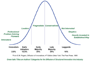
Interestingly, despite innovation being such a key to differentiation and value creation, there can be a wide range in the adoption of new innovations, as seen in Fig. 12.

Figure 1: Typical diffusion and adoption of innovation into industry
Having established how important innovation can be to successful enterprises, let us focus now on the topic at hand – what are those 3 tricks to semiconductor device innovation. Well, sorry to disappoint you but there are actually no easy tricks. And now that I have your attention, let me start by debunking a few myths.
Device Innovation: some True Lies
First, there is nothing magical about semiconductor device innovation. A second myth is that innovation is some sort of a Eureka moment. For thousands of years, humans have believed in the fallacy that innovation occurs like a lightning-strike of brilliance. It is generally believed that: 1) a person must passively wait for breakthrough ideas to hit and cannot take direct control of the creative process; 2) any person lucky enough to receive a significant idea must grab the most benefit possible because lightning-strikes of brilliance may never reoccur; 3) finally, serial innovators and inventive geniuses are rare talents. All these concepts are flawed. Much like other innovations, semiconductor device successes have instead been a product of structured innovation at its best.
Device Innovation: the gift that keeps on giving
Device innovation is often a virtuous cycle of continuous co-optimization of 3 key ingredients: materials, stack/device structure and device electrical operation. You start with materials which determine what is possible. Then you optimize the device structure to build what is manufacturable and finally you tune the electrical operation to ensure that the device stays reliable over its product life. As an example, you can breathe on a wafer and create a native oxide device that can even switch between 2 memory states. Question is whether it will switch reliably over a billion plus cycles and meet present day performance, manufacturability and cost criteria. A structured innovation cycle of co-optimization of these 3 criteria is the methodology that needs to be repeated diligently till the device Key Parametric Indices (KPIs) are met. As an example, Intermolecular has successfully demonstrated use of its device innovation capabilities in such a virtuous cycle to realize many leading-edge memory and selector devices across various materials systems. This wheel of materials and device innovation is illustrated below in Fig. 2 below:

Figure 2: Device innovation powered by co-optimization of materials, electrical operation, and device structure to meet device KPIs.
Its very foundation is the co-optimization of materials, device structure, and device operation which is achieved by rapid combinatorial depositions, advanced physical and electrical characterizations, data analysis to assess device performance and reliability, and an ongoing understanding of mechanisms that drive device behavior.
Semiconductor Devices: The heat is on
Not so surprisingly, technical progress in the semiconductor industry follows a “method to the madness”. For semiconductor products, it starts with an application that drives software and system architecture which in turn drives chip architecture to devices to process integration to materials. For successful device innovations, it is essential to understand the metrics that drive device behavior. Emerging and leading-edge logic and memory devices are a co-optimization and improvement on the following parameters listed in Table 1:

Table 1: Exemplary leading-edge parameters (KPIs) that drive device innovations
Device innovation: a case study is worth a thousand words
Next, let us review a case study which will further underscore the methodology of co-optimization describe in section 3 to achieve KPIs as illustrated in section 4. A few years ago, a leading-edge memory maker approached Intermolecular to find a selector device that would have best in class performance for all the parameters in Table 1’s emerging selectors column. The material system for this Ovonic Threshold Switch (OTS) diode was expected to be a multinary (3 to 7) chalcogenide elements. While each of those parameters are extremely difficult, a major “stone wall” was a trade-off between leakage (IOFF) and thermal stability (Fig. 3)

Figure 3: Fundamental leakage versus thermal stability trade-off for OTS selectors
The technical team took on this challenge by simultaneously considering and co-optimizing the materials system based on co-ordination number and electrical bandgap, careful management of electrical compliance during operation, leveraging the device structure’s thermal conduction properties, underlying mechanisms understanding and last but not the least, machine learning to leverage the diversity and the quantity of the rich data set. As a result, over a 3 year period, as shown in Fig. 4, the device’s multinary material system was significantly improved to address device level KPIs such as leakage, thermal stability and furthermore, a chip physical design parameter such as threshold voltage drift (VTH).

Figure 4: Optimizing multinary elements (A to E) for device and design KPIs
Systems to chip design to devices to materials: that is how the cookie crumbles
With device innovation at its core, present day technology development focuses on emerging methodologies that extends device and materials technology co-optimization even further to higher orders of abstraction. Such leading edge technology development strategies involve including design interdependencies aka DTCO (Design – Technology Co-optimization) and some are stretching the optimization to include product and systems level careabouts such as with STCO (System – Technology Co-optimization). Following is what our key leading edge customers are highlighting as their focus areas. Fig. 5 shows TSMC’s3 estimates of the increasing DTCO contribution at each node versus traditional scaling that is independent of co-optimization with chip design.

Figure 5: Growing contribution of DTCO vs technology node
Similarly, Micron4 expects improved R&D efficiency and value to their end customers when a wholistic approach to technology optimization includes chip design, packaging and product level interdependencies, as seen in Fig. 6.

Figure 6: Wholistic approach that includes product, design, package, process and device interdependencies for improved R&D efficiency and value generation
Semiconductor Devices: to infinity and beyond
The global semiconductor industry is anticipated to grow to US$1 trillion in revenues by 2030, doubling in this decade5. This will be enabled by innovations in devices and materials at its core. The Roadmaps of the Electronics industry underscore this target rich landscape and a bright future for semiconductor devices. So don’t stop thinking about tomorrow and be a device innovator now and forever. Each one of us will be a contributor to this incredible progress either as the innovator, the maker or perhaps even a user of the semiconductor devices. As these emerging devices not just survive but actually thrive, I invite you to embrace structured innovation and leave Eureka to just being a coastal city in Humboldt County, California.
References:
- https://www.rollingstone.com/culture/culture-news/steve-jobs-in-1994-the-rolling-stone-interview-231132/
- Silicon Valley Engineering Council (SVEC) Journal, Vol. 2, 2010 pp 38-71.
- Mark Liu, TSMC, ISSCC – International Solid-State Circuits Conference, 2021
- S Deboer– Micron, Tech Roadmap, November 2020 https://www2.deloitte.com/us/en/pages/technology-media-and-telecommunications/articles/semiconductor-industry-outlook.html
About EMD Electronics
EMD Electronics is the U.S. and Canada electronics business of Merck KGaA, Darmstadt, Germany. EMD Electronics’ portfolio covers a broad range of products and solutions, including high-tech materials and solutions for the semiconductor industry as well as liquid crystals and OLED materials for displays and effect pigments for coatings and cosmetics. Today, EMD Electronics has approximately 2,000 employees around the country, with regional offices in Tempe (AZ) and Philadelphia (PA).
For more information, please visit www.emd-electronics.com.
About Merck KGaA, Darmstadt, Germany
Merck KGaA, Darmstadt, Germany, a leading science and technology company, operates across life science, healthcare, and electronics. More than 64,000 employees work to make a positive difference to millions of people’s lives every day by creating more joyful and sustainable ways to live. From providing products and services that accelerate drug development and manufacturing as well as discovering unique ways to treat the most challenging diseases to enabling the intelligence of devices – the company is everywhere. In 2022, Merck KGaA, Darmstadt, Germany, generated sales of € 22.2 billion in 66 countries. The company holds the global rights to the name and trademark “Merck” internationally. The only exceptions are the United States and Canada, where the business sectors of Merck KGaA, Darmstadt, Germany, operate as MilliporeSigma in life science, EMD Serono in healthcare, and EMD Electronics in electronics. Since its founding in 1668, scientific exploration and responsible entrepreneurship have been key to the company’s technological and scientific advances. To this day, the founding family remains the majority owner of the publicly listed company.
Also Read:
Investing in a sustainable semiconductor future: Materials Matter
LIVE WEBINAR: New Standards for Semiconductor Materials
Step into the Future with New Area-Selective Processing Solutions for FSAV
Share this post via:


Comments
There are no comments yet.
You must register or log in to view/post comments.