Area selective processing (ASP) is assuming ever greater importance in semiconductor fabrication. ASP involves deposition and removal of materials at the molecular level¾10 nm or less. Key applications of ASP include self-aligned contacts and fully self-aligned vias (FSAVs), scaling boosters that are essential to continue device shrinkage. By supporting techniques like metal-recess flows and dielectric-on-dielectric (DoD) flows, ASP can provide the tools needed for the semiconductor industry to stay on the roadmap.
Executing these precision fabrication steps requires very tight control of deposition and etch. These are complex processes with challenging chemistries. By addressing those issues, EMD Electronics, a business of Merck KGaA, Darmstadt, Germany, and its integrated portfolio of companies, provides a complete solution that enables semiconductor companies to build innovative devices.
Paths to ASP
Just as different types of photoresists have been formulated for conventional wafer patterning, so different ASP approaches have been developed to perform different tasks in additive fabrication.
· Intrinsically Selective Molecules
Intrinsically selective molecules are molecules engineered to aggregate on specific materials, such as metals only or dielectrics only. They can be used for selective deposition or for selective epitaxial growth. Applications include the growth of silicon germanium (SiGe) source/drains for logic or memory transistors, or Si/SiGe stacks for nanosheet gate-all-around (GAA) transistors.
· Small-Molecule Inhibitors
As the name suggests, small-molecule inhibitors discourage molecules from depositing on a surface. They are typically used to prepare nonplanar surfaces for the pattering of very small structures. The approach enables more aggressive scaling of design rules, which might otherwise be limited by gate-to-source/drain spacing and metal fill.
· Self-Assembled Monolayers
Self-assembled monolayers (SAMs) can be spun on or applied using vapor-phase deposition. These precisely assembled layers are used for selective capping of the top or bottom of fine structures such as lines and spaces or vias. SAMs enable bottom-up fill of advanced-node trenches or vias.
· Atomic-Layer Etching
Being able to precisely remove material is just as important as being able to precisely deposit it. Atomic-layer etching (ALE) enables the removal of monolayers of material. Applications include thickness reduction of DRAM dielectrics and cleanup steps like reactive ion etching (RIE). Atomic-layer etch is also used to create SiGe recesses in GAA transistors or to etch away other metal recesses.
EMD Electronics participates in all these areas.
ASP in action¾fully self-aligned vias (FSAVs)
FSAVs provide a good example of how ASP is being used to support device scaling. FSAVs are vias aligned with lines during the fabrication process through successive deposition and etch. It’s an effective approach but depends upon accurate positioning. Beyond the 3-nm node, edge placement errors (EPEs) from one layer to the next can be a problem. Now, the via is too close to the adjacent line. In extreme cases, copper can diffuse to the adjacent line, causing a short.
Reducing the width of the via in the next layer can help prevent this but the trade-off is increased resistance, with heat generation and greater power consumption, as well as RC delay. The alternative is to widen the spacing. This can be done in one of two ways: metal-recess flow and dielectric-on-dielectric (DoD) flow.
Metal-recess flow is an ASP step based on precision removal. It begins post CMP with a highly controlled etching step to create recesses in the copper (see figure 1). A second precision etch step cleans up the slides of the barriers down to the dielectric. Finally, the next layer of copper is deposited. The metal recess step increases the spacing between the via and the adjacent line.

Figure 1: Edge placement errors (EPEs) that reduce spacing between vias and adjacent lines can enable copper to diffuse across to the adjacent line, causing a short. In metal-recess flow, recessing the copper lines increases the distance between the via and the interconnect (right), preventing diffusion.
The DoD flow process requires both precision deposition and precision removal. In the DoD flow process, an inhibitor SAM engineered to grow on the copper but not the dielectric is grown on the metal (see figure 2). Next, a dielectric layer is deposited on the existing dielectric¾but the inhibitor layer prevents the growth of dielectric on the copper. After deposition, the inhibitor layer is removed from the copper. The cycle finishes with the growth of the next layer of via. Once again, the spacing between the via and the adjacent line has been increased using ASP.
Note that the dielectric-on-dielectric layer remains even after removal of the inhibitor layer.

Figure 2: In the DoD flow process, a copper-selective inhibitor (gray) is grown on the copper (brown). These features make it possible to deposit a dielectric layer (green) on top of the existing dielectric (blue). Once the inhibitor is removed from the copper, the next layer of via is deposited. Once again, the space between the via and the adjacent line is extended.
The fully self-aligned via (FSAV) process with ASP presents a few challenges:
- DoD Process:
- Materials: Developing a SAM selective for copper
- Process conditions: High temperatures can degrade SAM molecules, but atomic-layer deposition (ALD) traditionally yields the best quality dielectric thin films at higher temperatures.
- Chemistry: The halogen and oxygen precursors typically used for silicon dioxide (SiO2) ALD can damage the SAM, so we need halogen-free precursors and milder oxidants such as water.
- ALE of copper is a multistage process requiring complex chemistry. The first stage involves chemically modifying the copper. The second stage actually removes the modified copper.
EMD Electronics has the answers
We specialize in sophisticated chemistries and can draw on the resources of our integrated solutions across the organization. This has enabled us to solve the core challenges across the process.
- Materials: We’ve developed a SAM molecule that is copper selective.
- Process conditions and chemistry: We’ve developed a reduced-temperature ALD based on a halogen-free silicon precursor with water as the oxidant. Despite running at lower temperatures, the process yields high quality dielectric films (dielectric constant ≤ 5; leakage current ≤ 5e-7A/cm2), without damaging the SAM molecules.
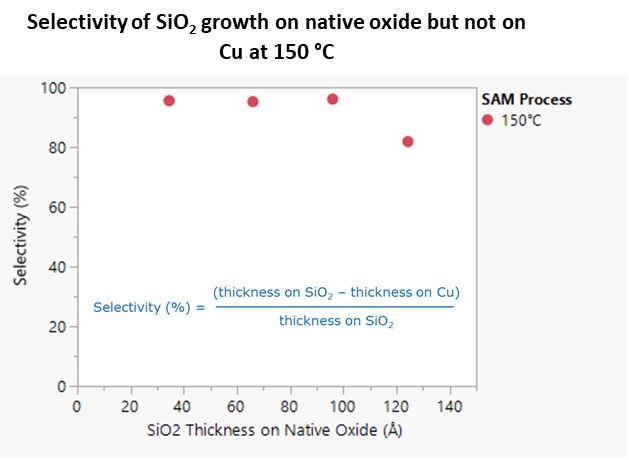
- DoD Selectivity: as a result of the above-mentioned material and process development, we are able to demonstrate selectivity of deposited SiO2 film up to ~10nm for deposition on SiO2 and minimal, if any, deposition on copper (figure 3)
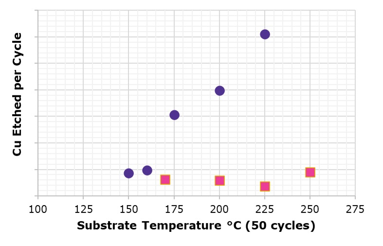
- Chemistry: By optimizing the molecular composition of the chemistry and the copper modification stage of our ALE process, we have demonstrated effective and highly controlled copper removal with minimal added roughness. This is an important improvement over conventional processes, that allowed for atomic level control over copper etch rate (see figure 4).

Figure 3: DoD selectivity of >95% for deposited SiO2 film upto thickness of ~10nm on SiO2 but not on copper (Ref. G. Liu et al., ASD 2022 Conference)

Figure 4: Atomic level control over copper removal using our optimized ALE (blue) process , beginning at 170° C. Conventional ALE (pink) shows minimal removal of copper, regardless of process temperature.
Conclusion
ASP is an essential technology to equip the semiconductor industry to meet the challenges of the future. We used FSAVs here to highlight the power of ASP and our technologies but there are many other applications for this suite of processes in the semiconductor industry. ASP can be used for selective metal definition for source/drain. They can be applied to create an area-selective copper line barrier, for example, or for metal-on-metal deposition, such as a cobalt cap.
EMD Electronics supports the full ASP process, from the SAMs required to protect the surface to the precursors of processes required to deposit materials at low temperatures to the specialty processes needed to etch away inhibitors. We have novel chemistries to address the challenges. We have processes and chemistries optimized to work together. Most of all, we have an organization that delivers vertically integrated support for development, problem-solving and innovation.
Also Read:
Integrating Materials Solutions with Alex Yoon of Intermolecular
Ferroelectric Hafnia-based Materials for Neuromorphic ICs
Webinar: Rapid Exploration of Advanced Materials (for Ferroelectric Memory)
Share this post via:


Solving the EDA tool fragmentation crisis