The ferroelectric effect in materials has been exploited to fabricate (fab) reliable Ferroelectric Random Access Memories (FRAM) Non-Volatile Memory (NVM) ICs for over 20 years. Recent years have seen have seen a breakthrough in discovering ferroelectric properties in Hafnium Oxide (HfO2 or “hafnia”), a fab-friendly material unlike previous perovskite-based materials like Lead Zirconate Titanate (PZT). This has the potential to revolutionize on-chip memory technology and to enable next-generation technologies such as artificial synapses for compute-in-memory (CIM) type neuromorphic ICs.
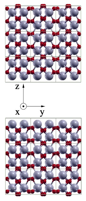
Crystals are ordered solids, as opposed to amorphous solids like glasses and plastics. The characteristics of a crystal–electrical, mechanical, optical, etc.–change when atoms line up to form interlocking grids, and many materials can solidify into different crystal forms. Pure carbon can be structured to be conducting soft dark graphite or insulating hard transparent diamond. Some complex crystals have polar atoms spaced so that a switching external electric field causes an internal shift of some atoms in the crystal lattice. This creates an electrical charge dipole giving rise to ferroelectric effects as shown in Figure 1.

PZT while used in ferroelectric memory devices is not fab friendly, and loses its ferroelectric properties when layers are very thin. Hafnia has been used as the storage capacitor in Dynamic RAM (DRAM) and as the gate dielectric in Logic ICs for many years due to its high dielectric constant and can maintain ferroelectric properties when ultra-thin. Typically, the ferroelectric phase of HfO2 is unstable. To stabilize the FE phase in HfO2, Zirconium (Zr) dopant has proven to be the most successful. As such, Hafnium Zirconium Oxide (HZO) has been one of the strongest FE material candidates for memory applications. Besides Zr, other dopants such as La, Y, Si, Gd have also been explored.
Material Deposition
Ferroelectric perovskites currently are deposited by sol-gel method or physical sputtering. However, these require high temperature anneals to achieve the ferroelectric crystal structure, but CMOS backend of line (BEOL) integration has a limited thermal budget of ~400°C. To achieve well controlled ultra-thin films in small, high density devices, advanced commercial IC fabrication relies upon atomic-layer deposition (ALD), specialty cleaning and surface treatments to ensure that all atoms line up where needed. Underlayers are prepared and cleaned to create optimal reaction surfaces. Then special ALD organometallic precursors are used to deposit desired materials one monolayers at a time.
ALD film composition and processes must be controlled to achieve the desired crystal orientation and inhibit the growth of all other thermodynamically possible orientations. Some precursors can deposit hafnia-based films with ferroelectric properties https://bit.ly/34AEFoJ but this is not always the case. With the right surface and the right process conditions, exposed surface atoms can provide a “template” to support the growth of the desired crystal orientation. The ferroelectric properties of HZO can also be improved by interface engineering, such as forming nanolaminates with distinct layers of HfO2 and ZrO2 https://bit.ly/3wLF0Rt). Rapid Thermal Anneal (RTA) can also drive the transformation to the ferroelectric phase.
Design and Reliability Considerations for Ferroelectric Memory
Ferroelectric memories can be three types, (i) FeRAM – a one transistor – one capacitor type device where the information is stored by modulating polarization capacitance, (ii) FeFET – a transistor with ferroelectric material as a gate dielectric where the threshold voltage is modulated based on the polarization, (iii) FTJ – a tunnel junction that stores information by modulating the tunnel barrier based on the orientation of the electric dipole polarization. FeRAM and FeFET historically have been more popular. Nevertheless, FeRAMs have destructive read process, and FeFETs are three terminal devices where the cycling endurance is critically dependent on the gate dielectric/semiconductor interface. Most importantly, neither of these is a resistive switching device that is essential for realizing synaptic devices for some neuromorphic computing architectures.

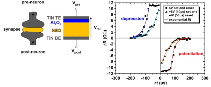
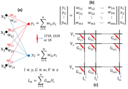
Neuromorphic computing can be broadly classified into two categories, (i) ones that aim to actively emulate human learning processes and behavior and (ii) ones that emulate the connectivity and information flow of the brain through artificial neural networks (ANN), but do not necessarily emulate human learning processes. One common embodiment of the former category is Spike-Timing Dependent Plasticity (STDP) that changes the weight of the synapse based on timing differences between the arrival of pre- and post-synaptic signals (See Fig. 2). In hardware implementations, the weight changes are stored in non-volatile memory devices like FTJ. ANN type computing is pervasive because it can be implemented in a CMOS hardware platform, and it has a flexible design methodology. Typical CMOS hardware is not adequate for storing and accessing the number of synaptic weights that are required for the state-of-the-art neural network models that rely on off-chip memory. Hence, a cross-bar array of analog non-volatile memory is used to enable CIM architecture which encodes the matrix-vector multiplication, a key component of both ANN learning and inference. [See Fig. 3].

FTJs with hafnia materials have the potential of becoming an ultra-low power memory for the CIM architecture, compatible with CMOS BEOL integration. A key remaining challenge is to maintain analog switching behavior as the FE domains get smaller with scaling. ALD deposition of inherently FE films can solve this problem by demonstrating FE behavior in ultra-thin films.
Just as thick PZT layers provide a foundation for reliable digital FRAM, thin HZO ferroelectric layers provide a foundation for ultra-low-power analog neuromorphic ICs. HZO monolayers hold information at the atomic level as artificial synapses to enable Artificial Intelligence (AI) and Machine Learning (ML) circuits as well as new Compute-In-Memory (CIM) architectures. HZO-based devices use “fab-friendly” materials such as TiN electrodes for low-cost and easy integration, enabling future cost-effective commercial fabrication of high-yielding neuromorphic chips.
Also Read:
Webinar: Rapid Exploration of Advanced Materials (for Ferroelectric Memory)
Executive Interview: Casper van Oosten of Intermolecular, Inc.
Integrating Materials Solutions with Alex Yoon of Intermolecular
Share this post via:


Solving the EDA tool fragmentation crisis